|
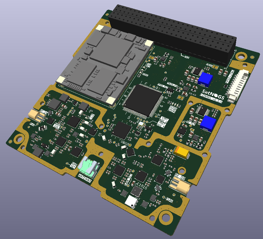
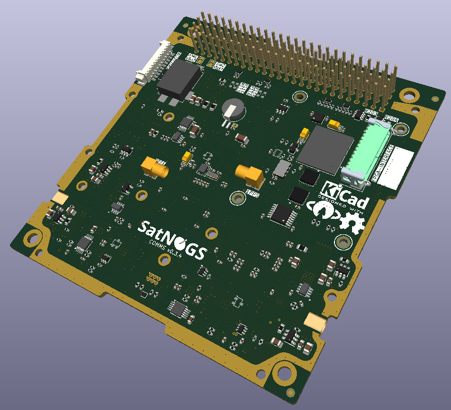
SatNOGS-COMMS
4.1.0
A COMMS subsystem for CubeSats
|
|
SatNOGS-COMMS
4.1.0
A COMMS subsystem for CubeSats
|
The user manual contains information about the handling, connections and necessary setup and tools required for the proper use of the SatNOGS COMMS board. Additionally, information about the flight model customization is provided in the appendix.
 | SatNOGS COMMS is and ESD sensitive device.Standard ESD handling methods should be followed when handling the PCB. Always use an ESD mat and ESD wristband. |
 | It is advised to wear gloves when handling the system to avoid contamination. Should cleaning of any parts is required, use ESD safe cleaning methods and non-reactive solvents. It is recommended to handle the unit in a clean environment using an appropriate laminar flow workbench or an ISO class 8 cleanroom. |
| | It is recommended to store in a controlled environment with temperatures between 15◦ C and 30◦ C, relative humidity of 40% to 65%, using appropriate packaging materials such as antistatic bags or moisture barrier bags with desiccants. |
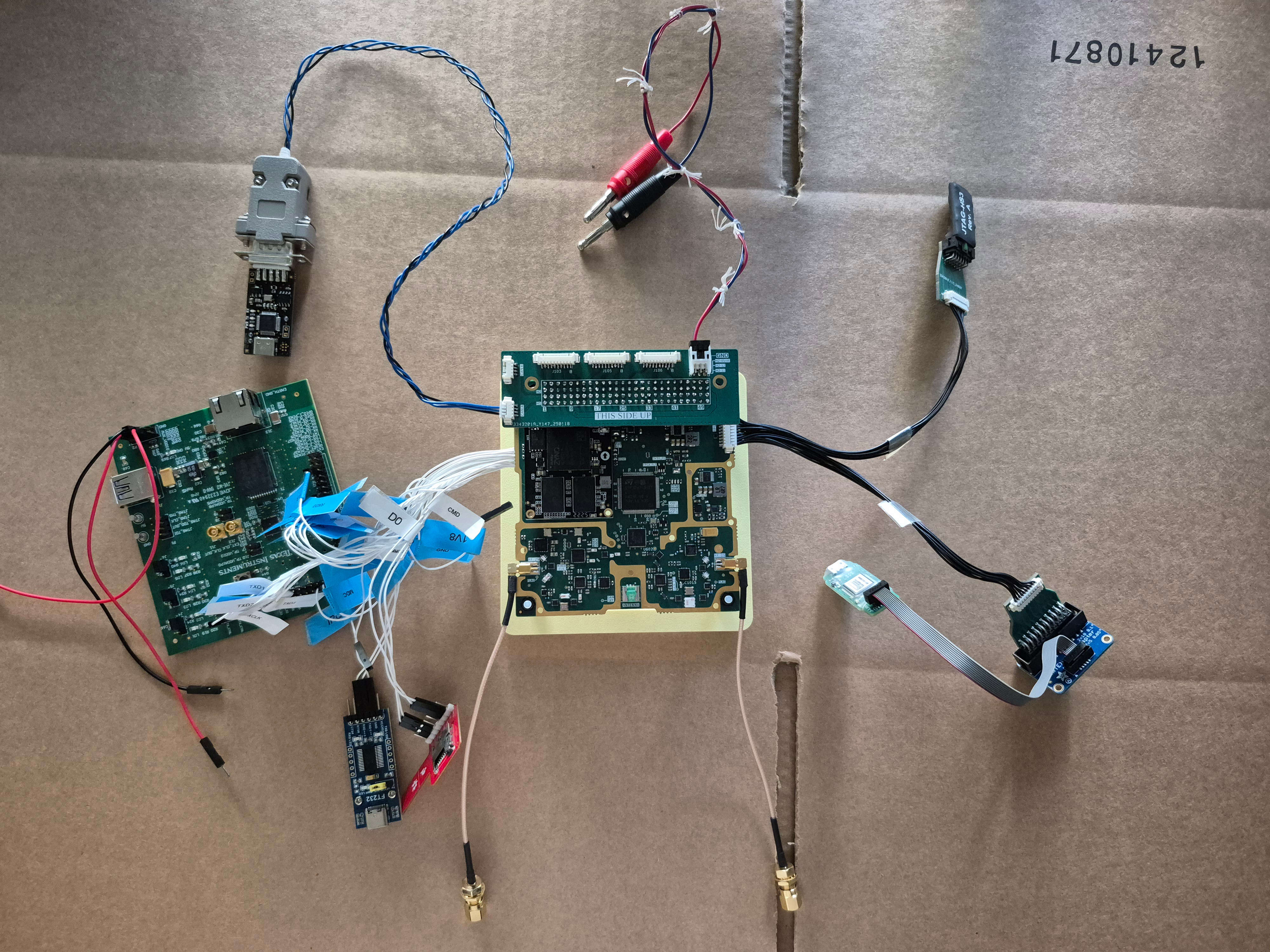
To operate the SatNOGS COMMS board on lab, the support equipment below is required.
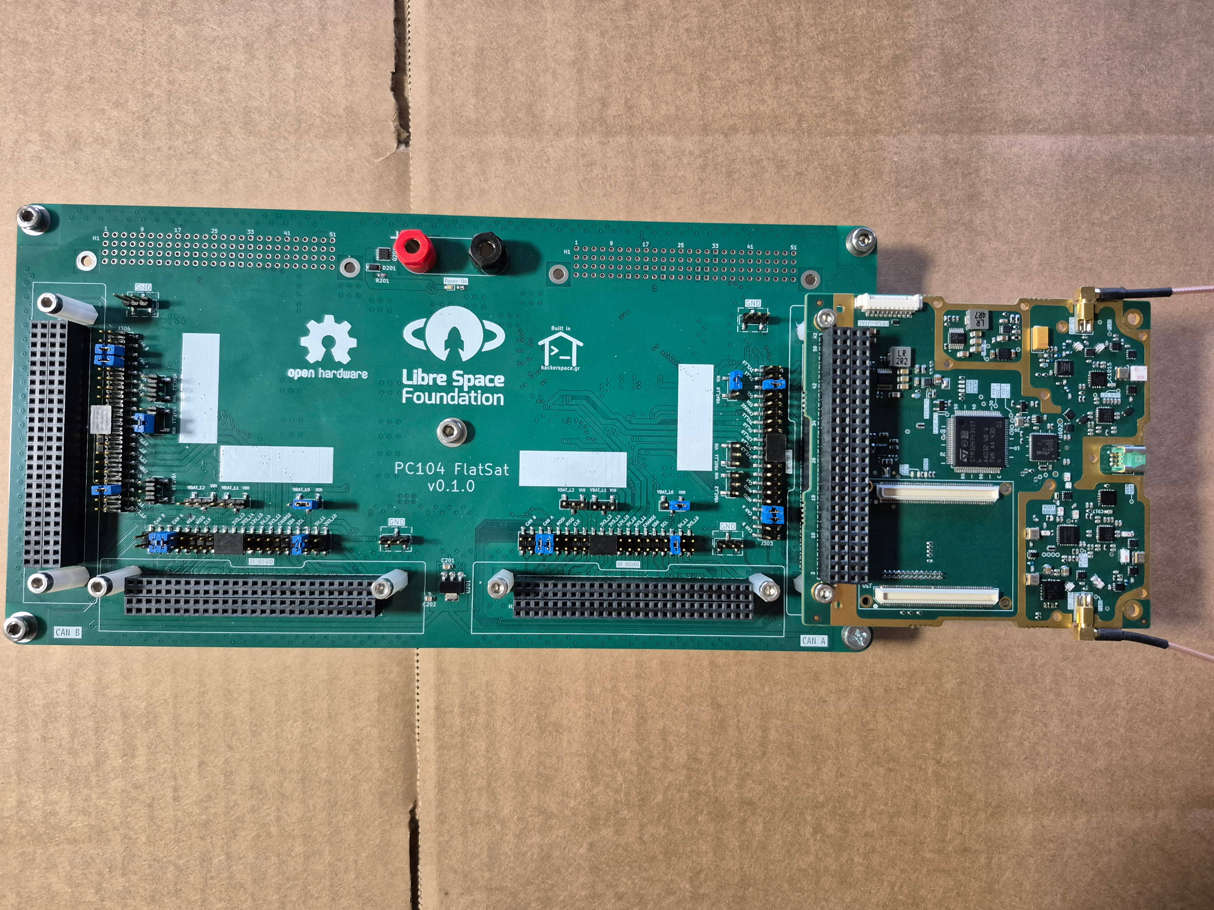
 | PC-104 FlatSat board |
 | PC-104 Breakout board |
 | Librecube mount |
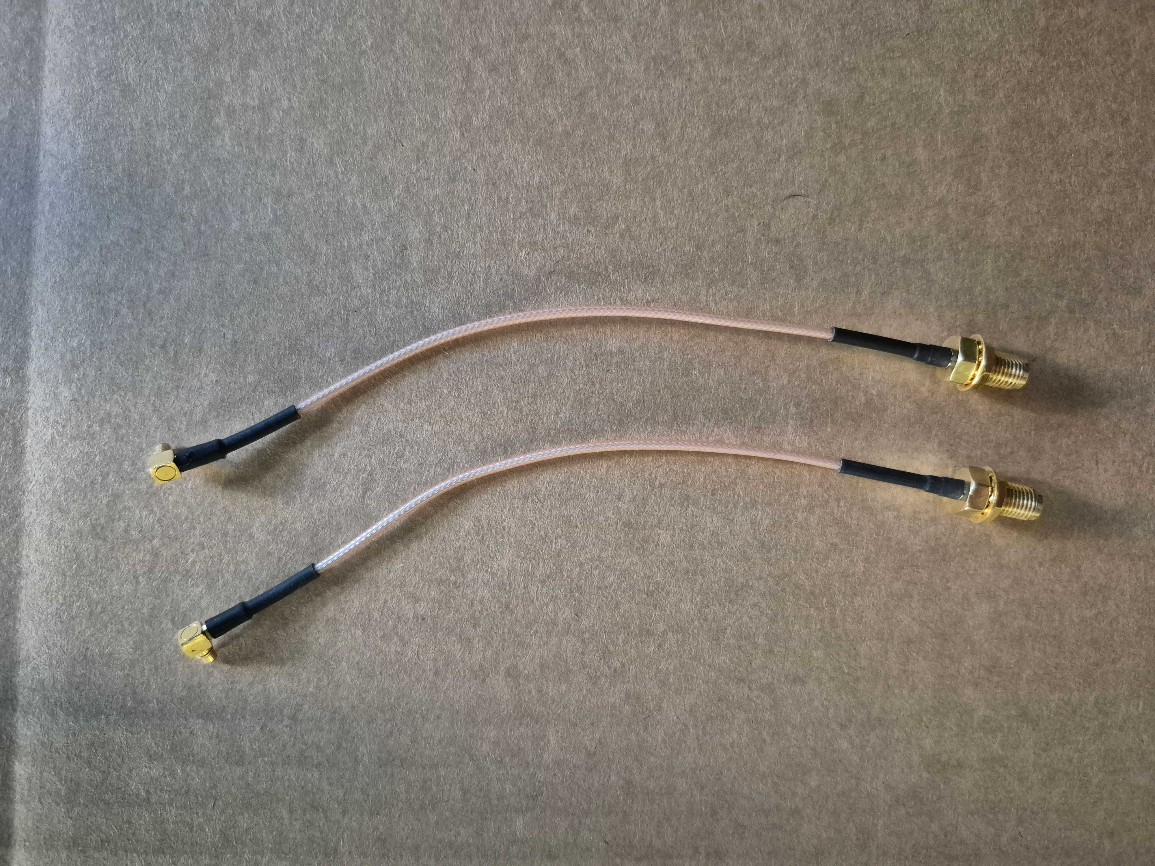 | 2 x MMCX to SMA RF Cables Note: CAB725RF-0150-00-A-1 or similar Optional Two RF cables for transceiver clock (RFFE) and FPGA clock (1PPS). |
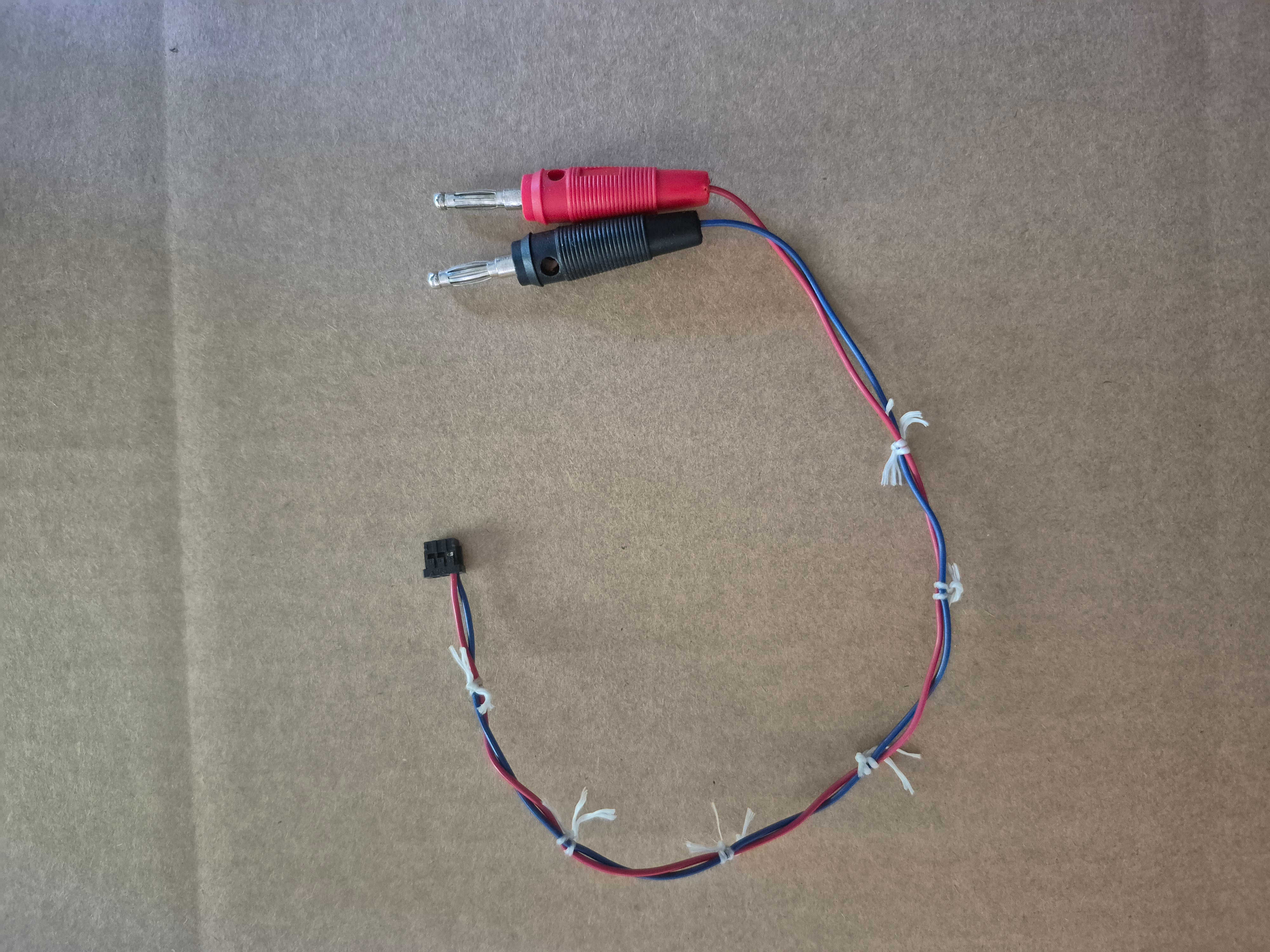 | PC-104 Breakout Power cable Note: DF11-6DS-2C to 4mm Banana plugs (Power Supply cable, Alpha Wire 3049, 26AWG recommended) |
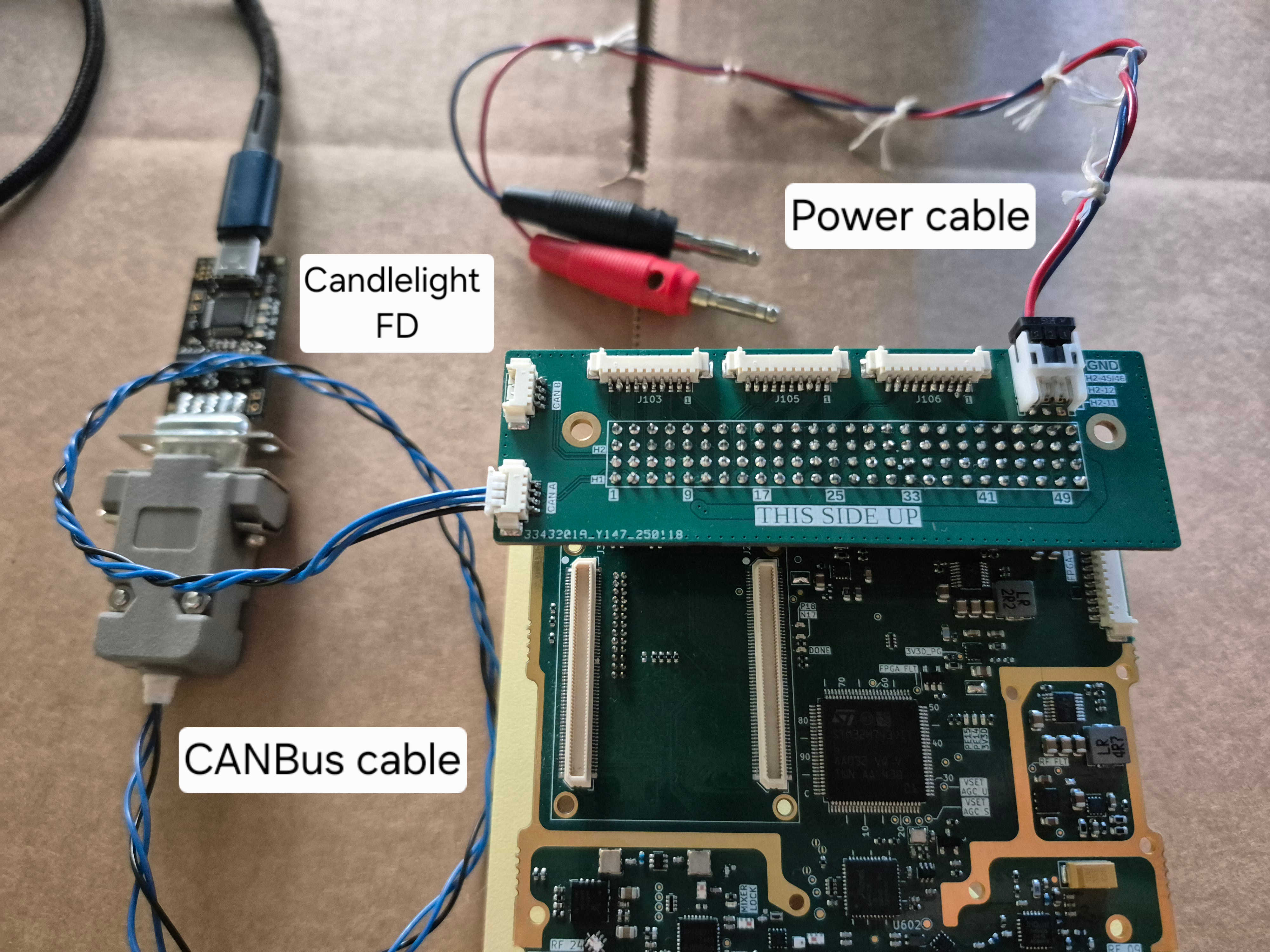
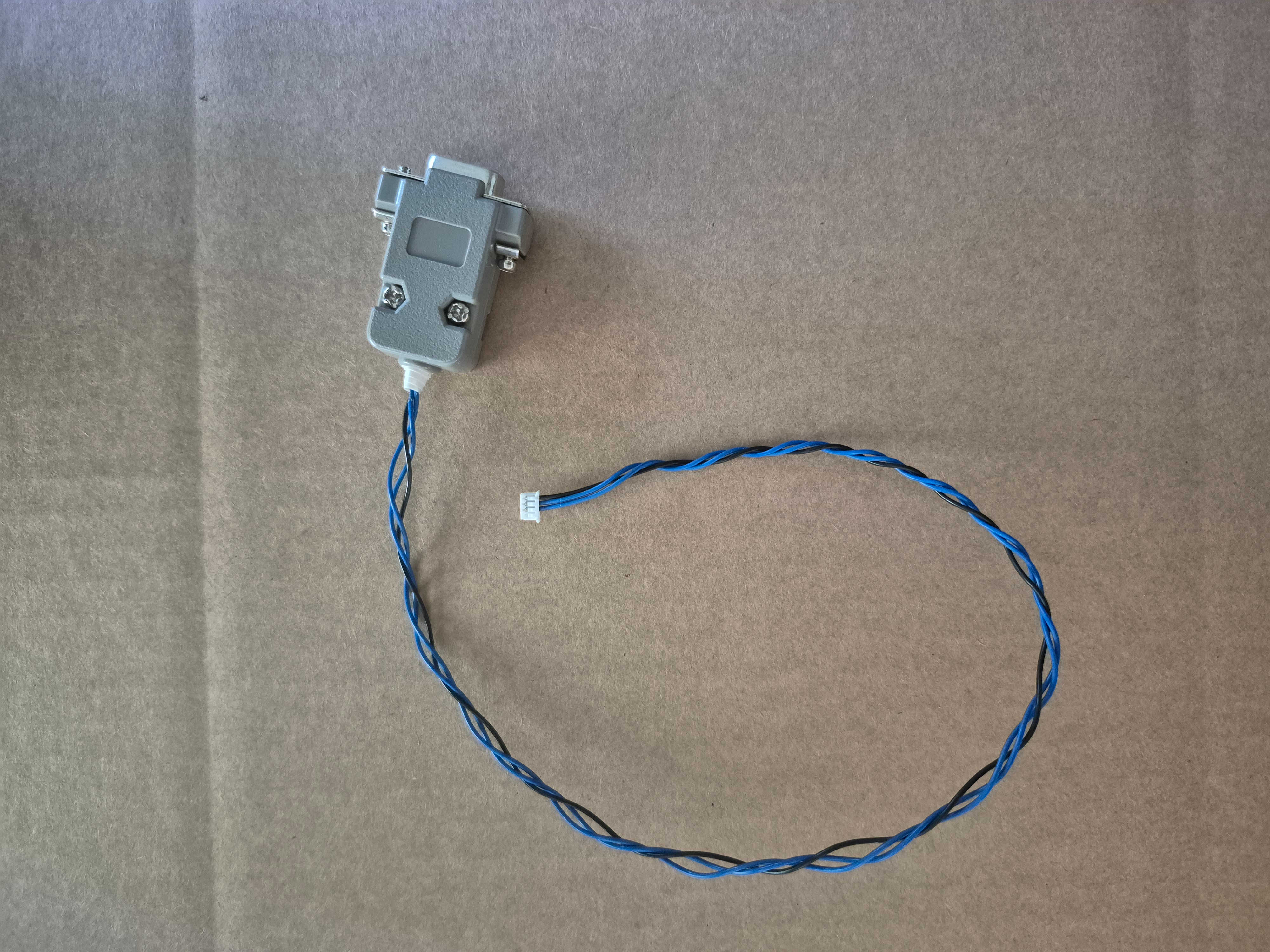 | CANBus cable Note: Molex PicoBlade 510210400 to DSUB-9 with backshell (CAN Bus cable, Alpha Wire 3049, 26AWG recommended) |
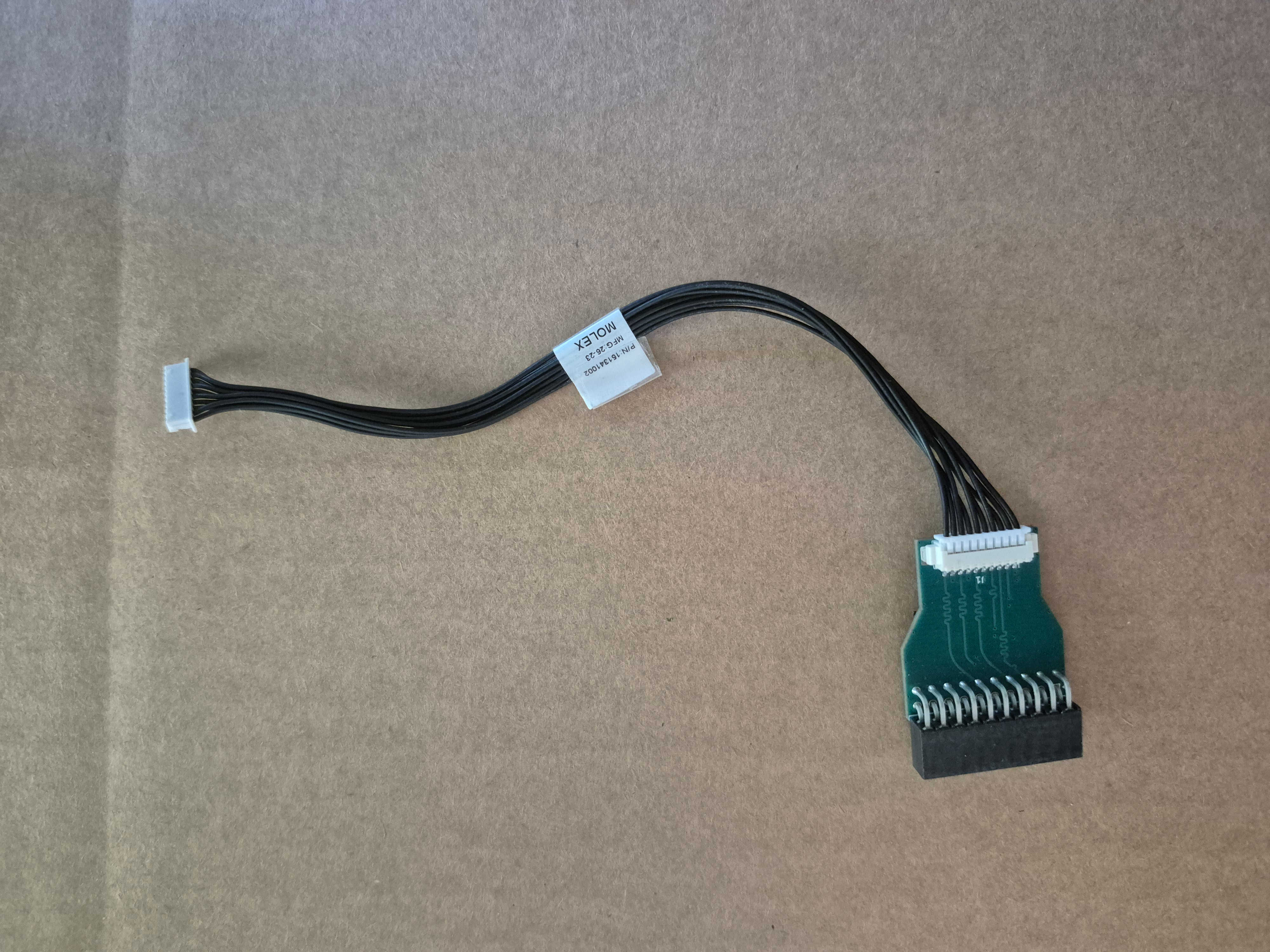 | MCU Programming breakout board with cable Note: Molex picoblade 151341002 connected to MCU Programming Breakout Board |
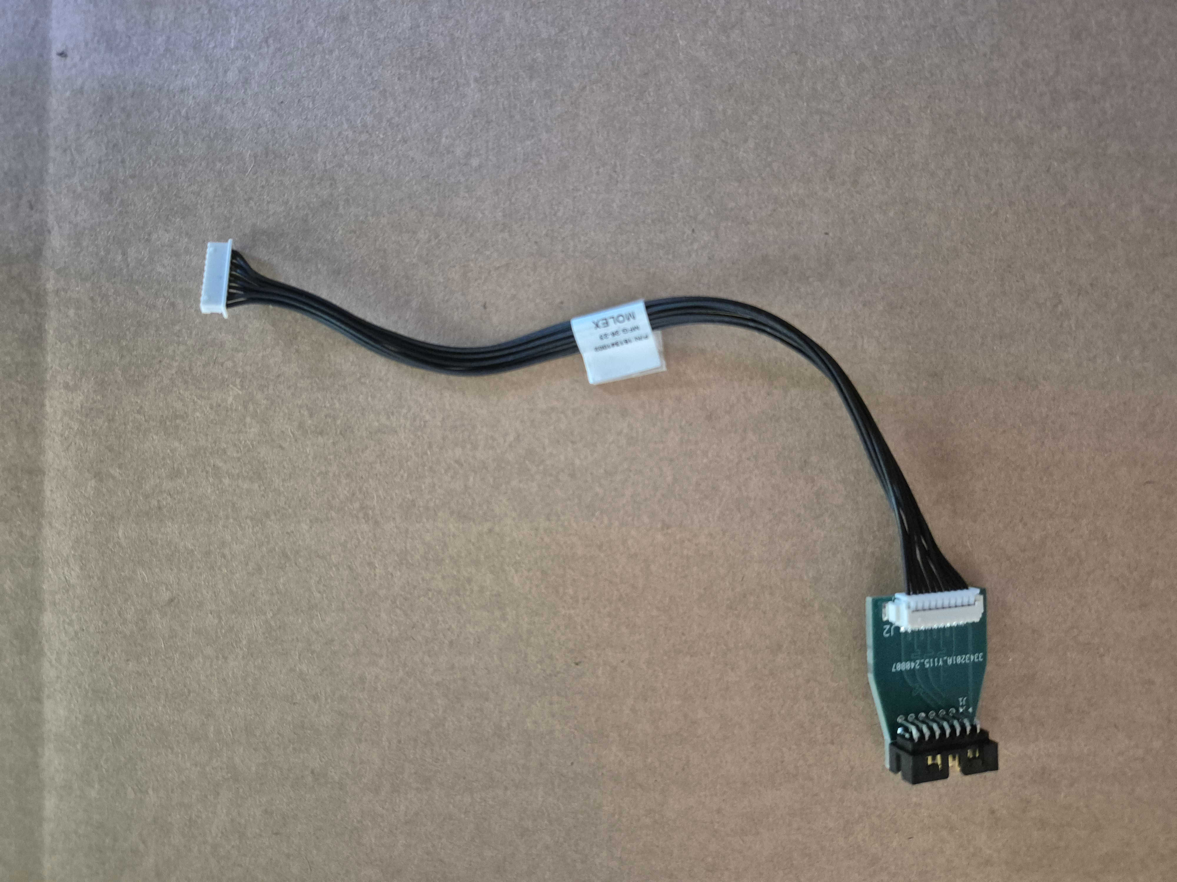 | FPGA Programming breakout board with cable Note: Molex picoblade 151341002 connected to FPGA Programming Breakout Board |
 | FPGA Interface cable Note: G125-FC12605L0-0150L with individual female dupont-style sockets M20-1160042 & M20-1060100 on pigtail end. |
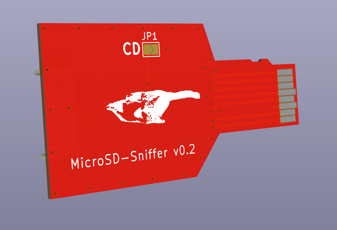 | eMMC sniffer board Alternative: MicroSD sniffer. |
 | CandleLight-FD |
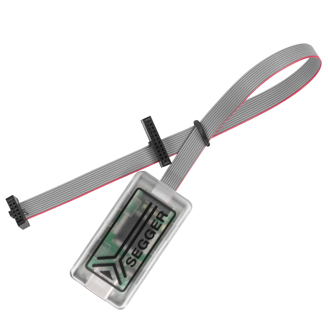 | JLink EDU Mini with 2094 Note: Segger™ JTAG EDU or STLINK/V2 |
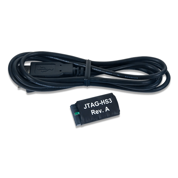 | JTAG-HS3 Note: XILINX Platform Cable USB with ribbon cable |
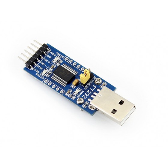 | UART to USB device Note: Waveshare FT232 or similar |
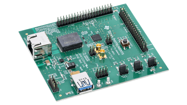 | DP83867ERGZ RGMII 1000M/100M/10M Ethernet PHY evaluation module Note: 5V on turret pins (5V and GND) 1.8V on P2 connector (Pin 3 = VDDIO EXT, Pin 7 = VDDA1P8) To use only external 1.8V, solder R77, R67, R68 and remove R74. |
The necessary connections of the ground support equipment are provided below.
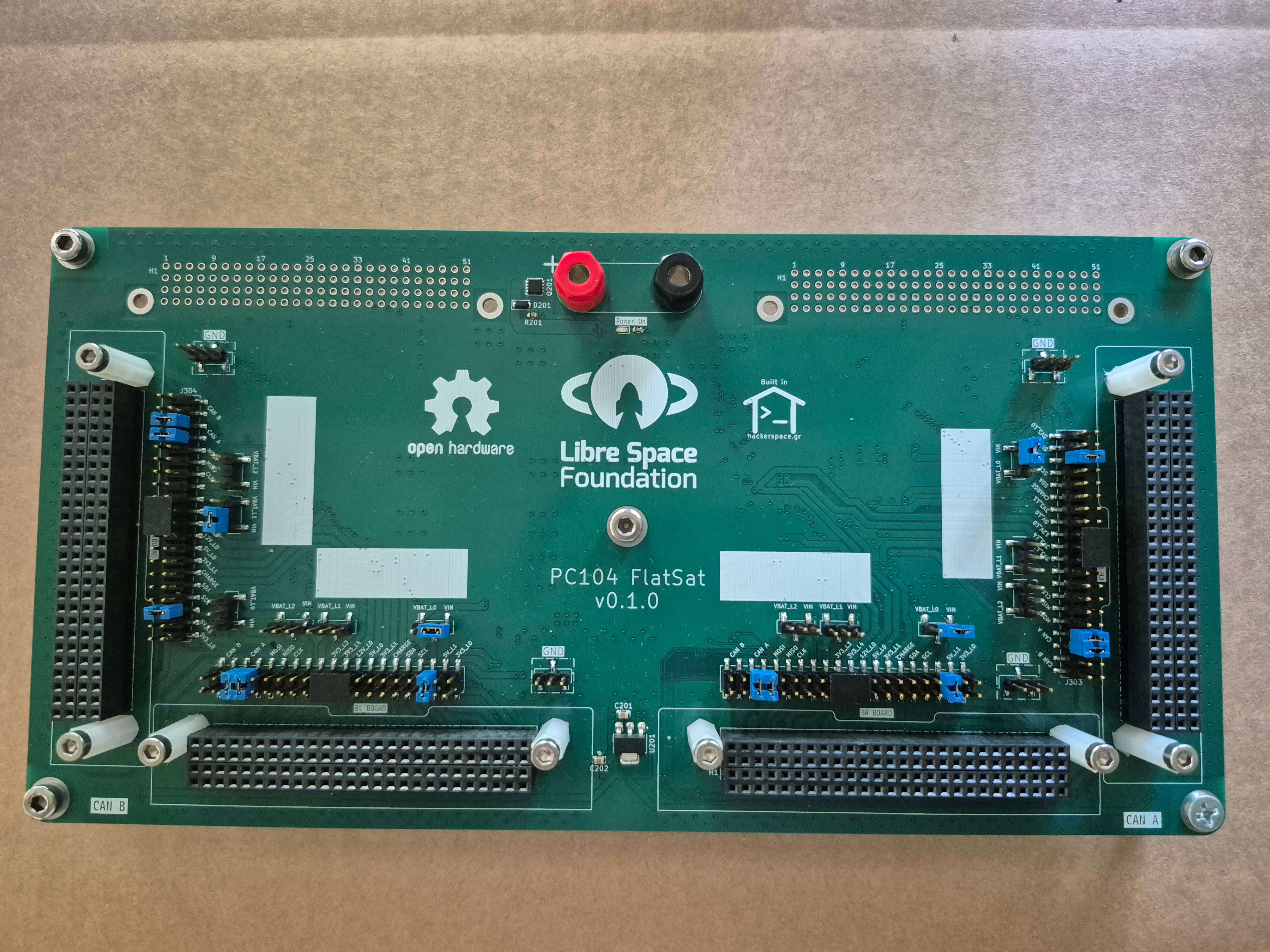
The PC104 FlatSat is a PCB designed to connect up to four PC104 subsystems for testing and debugging. The board can be powered via standard male banana plugs, with a default power setting of 12V/1A. As shown in Figure 2, the CAN bus interface is located on the bottom side of the board. To connect the subsystems together, place 2.54mm jumpers on the appropriate pins of the 20-pin connector located in front of each subsystem's PC104 connector. The power configuration can also be adjusted using 2.54mm jumpers on the 3-pin connectors positioned in front of those 20-pin connectors. A default configuration example is demonstrated in Figure 1.
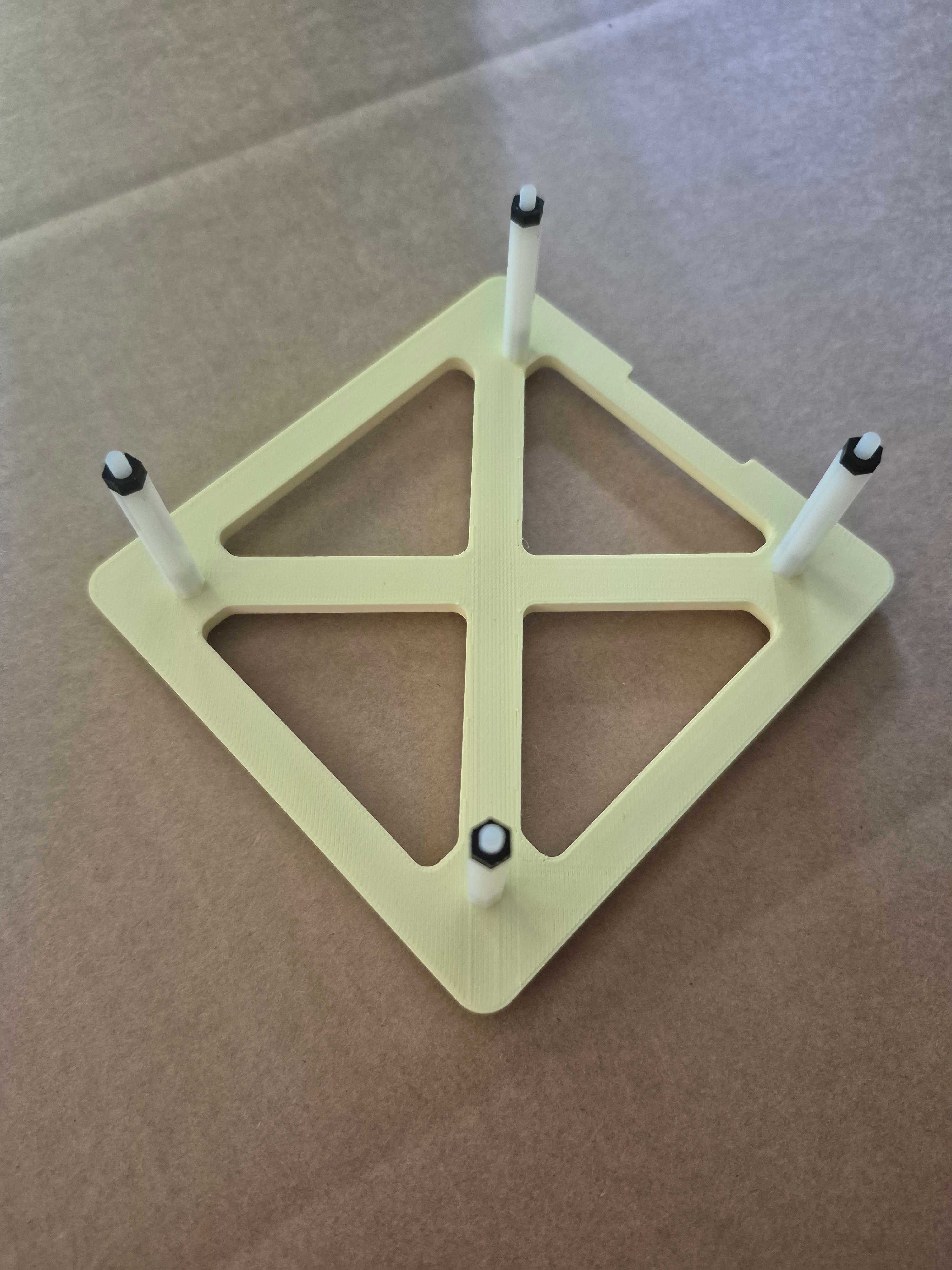
The LibreCube mount is a 3D-printed bracket designed to securely hold the SatNOGS COMMS board in place. Installation requires four M3 nuts and four M3 male/female standoffs, either 35mm or 45mm in length (part number: CBMFTS335A).
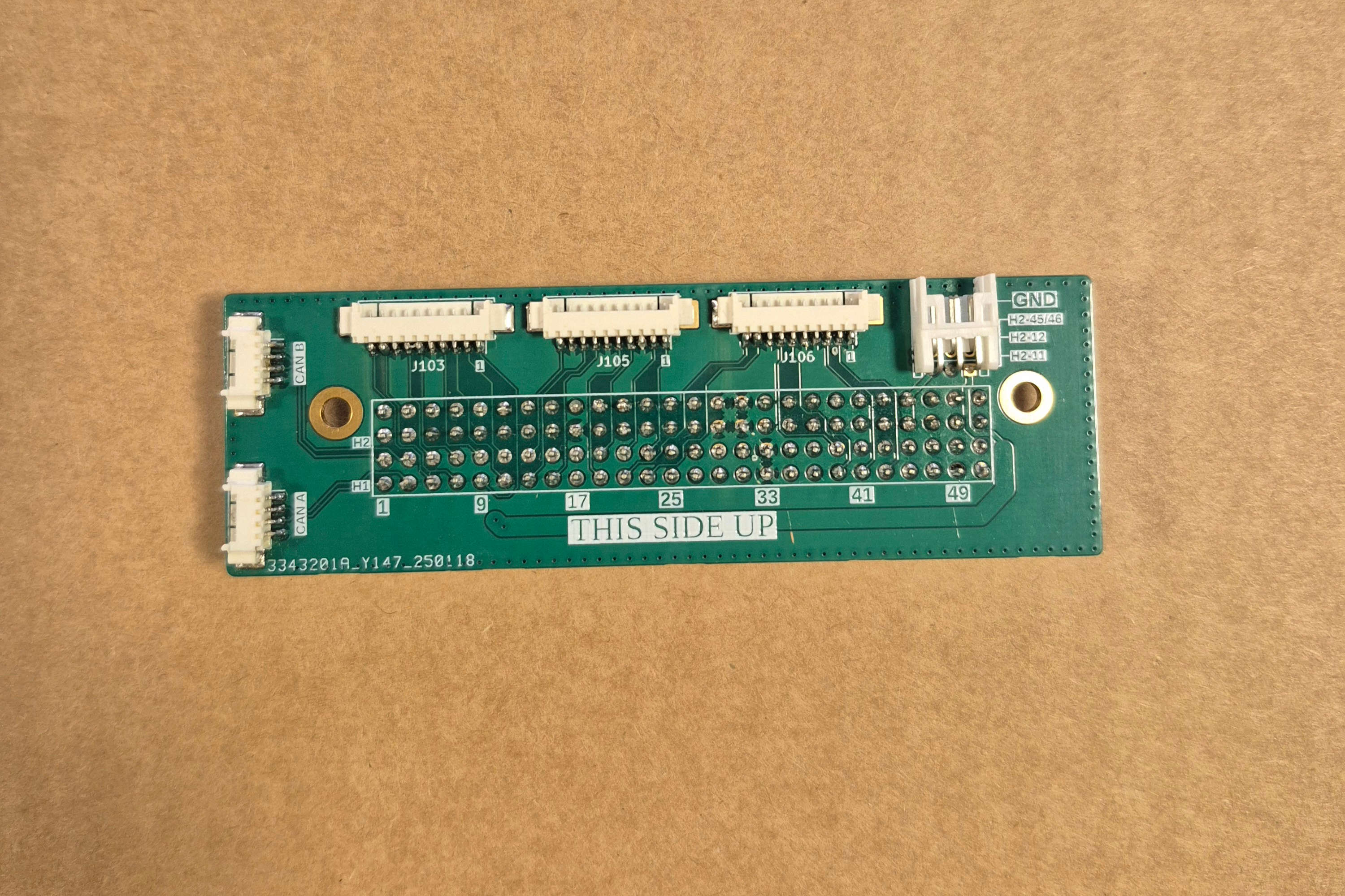
The PC104 breakout board is a PCB which fits on the top of the PC104 of the SatNOGS COMMS board and exposes the PC104 interface such as CAN, I2C, power etc. to individual connectors for easier and straigh-forward connection to the debugging devices. It can be used together with PC104 flatsat for multiple SatNOGS COMMS boards alignment.
SatNOGS COMMS can operate over a voltage range of 5.5V to 30V DC (for version 0.3.2 and above). This can be provided either through a power supply or directly from the satellite battery.
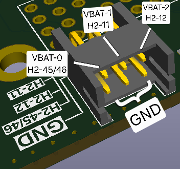
A power supply should be connected to VIN and GND pins as described in the Interface control document. Adjust the current limit so that a maximum power of at least 10W is available.
A typical setting of the power supply is 12V/1A.
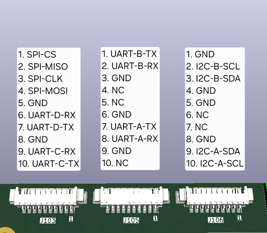
Viewing the breakout board from the top (THIS SIDE UP), the pinout of the Hirose DF13 power supply connectors is depicted in pc104-breakout-power Figure 5.
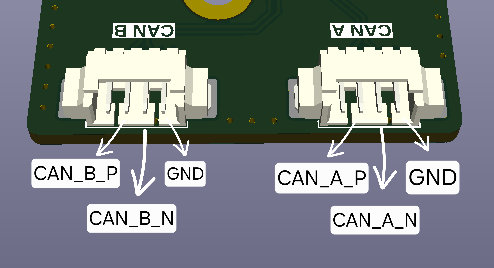
SatNOGS COMMS uses the CAN bus transceiver TCAN334G. The pins are exposed through the PC/104 interface as described in the Interface control document. The termination resistor is optional and tunable. Typically a value of 120Ω is used.
Viewing the breakout board from the top (THIS SIDE UP), the pinout of the Molex PicoBlade CAN connectors is depicted in pc104-breakout-can Figure 6.
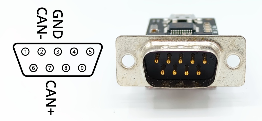
To read and send CAN messages from/to the board the candleLight FD USB to CAN adapter is used. For convenience during cable manufacturing or on-site cable repair, the connections on the device’s D-SUB 9 male connector are provided:
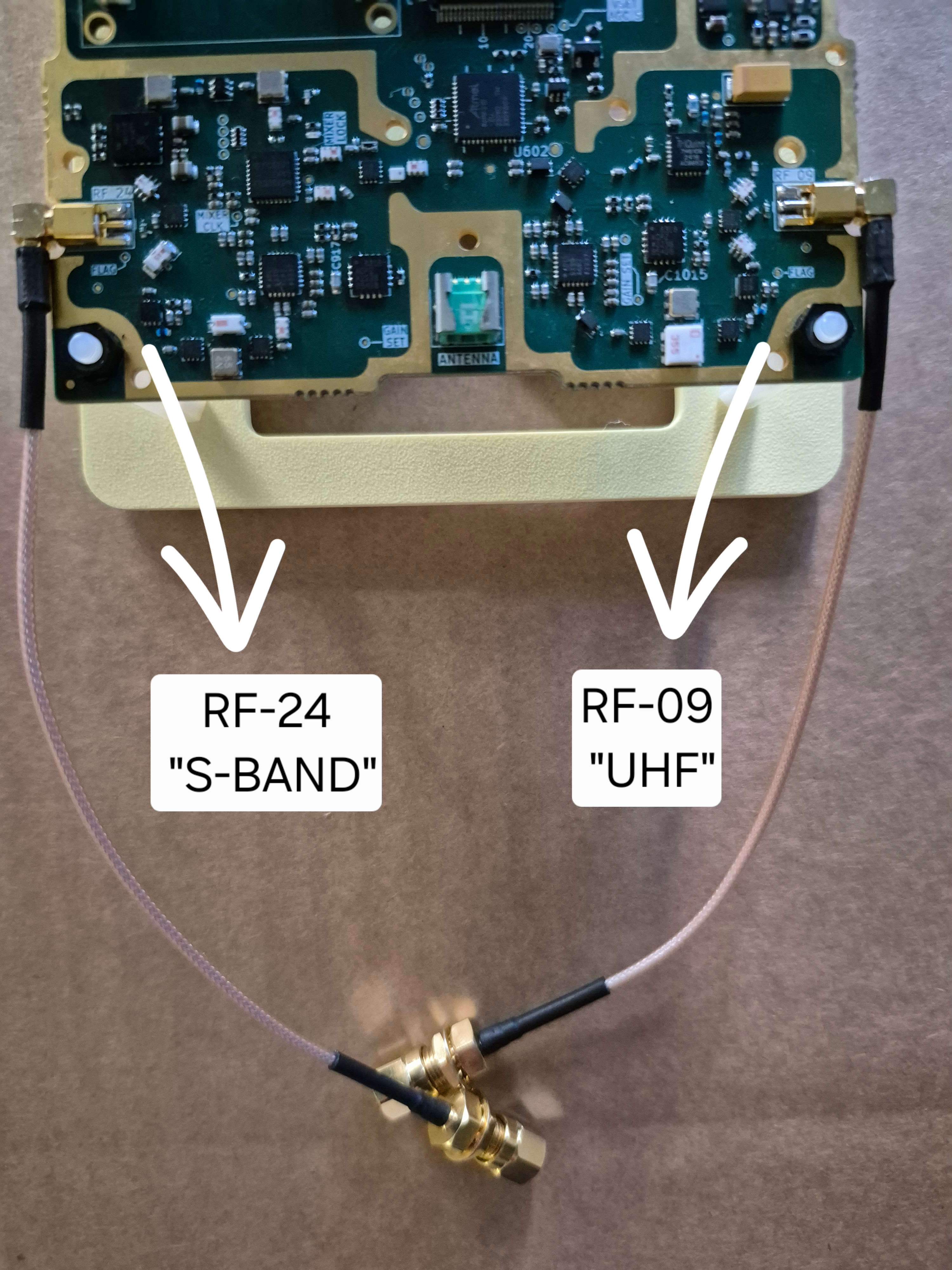
SatNOGS COMMS should always be powered with a 50 Ohm antenna or a 50 Ohm RF load capable of sinking 2W and operating at the design specific band connected to its RF ports. Failing to do so may result in catastrophic system failure.
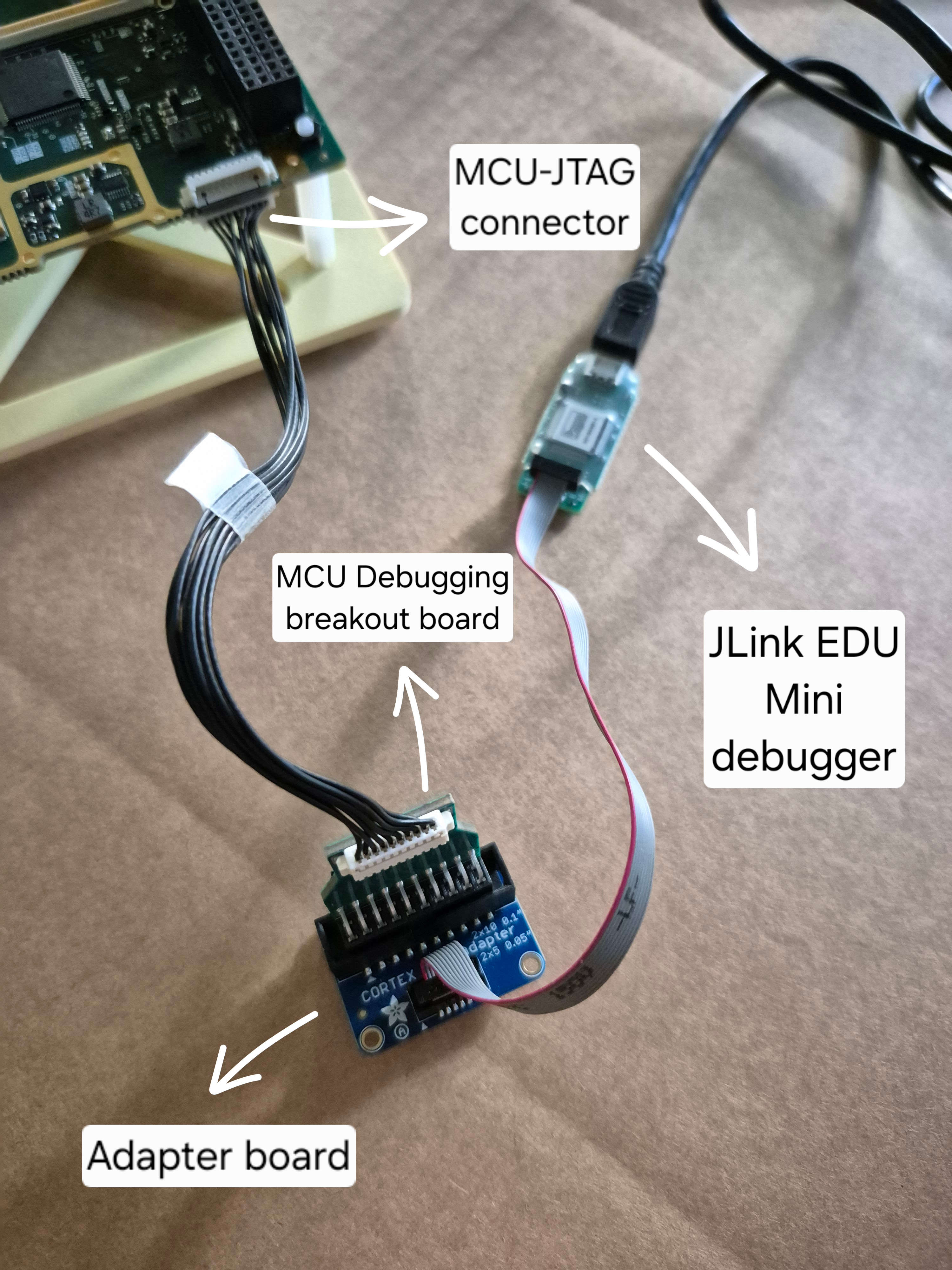
A 10-pin connector "MCU-JTAG" (53261-1071) is located on the bottom right side of the board for the debugging and programming of the STM32H743HI MCU as described in the Interface control document. Various devices that support JTAG programming can be used. A 10-pin female to pigtail cable assembly (2181121001) can be used to directly connect the board to a JTAG/SWD debugger by crimping the pigtail side to typical female pin strips.
Another option is to use a cable assembly, for example 151341002 connecting one side to the "MCU-JATG" connector and the other side to the MCU Programming Breakout Board, which can be connected directly to a JTAG/SWD debugger, for example Segger™ JTAG EDU or STLINK/V2, or connected to an adapter board (2094) which in turn is connected to a JTAG/SWD debugger, for example Segger™ JTAG EDU Mini.
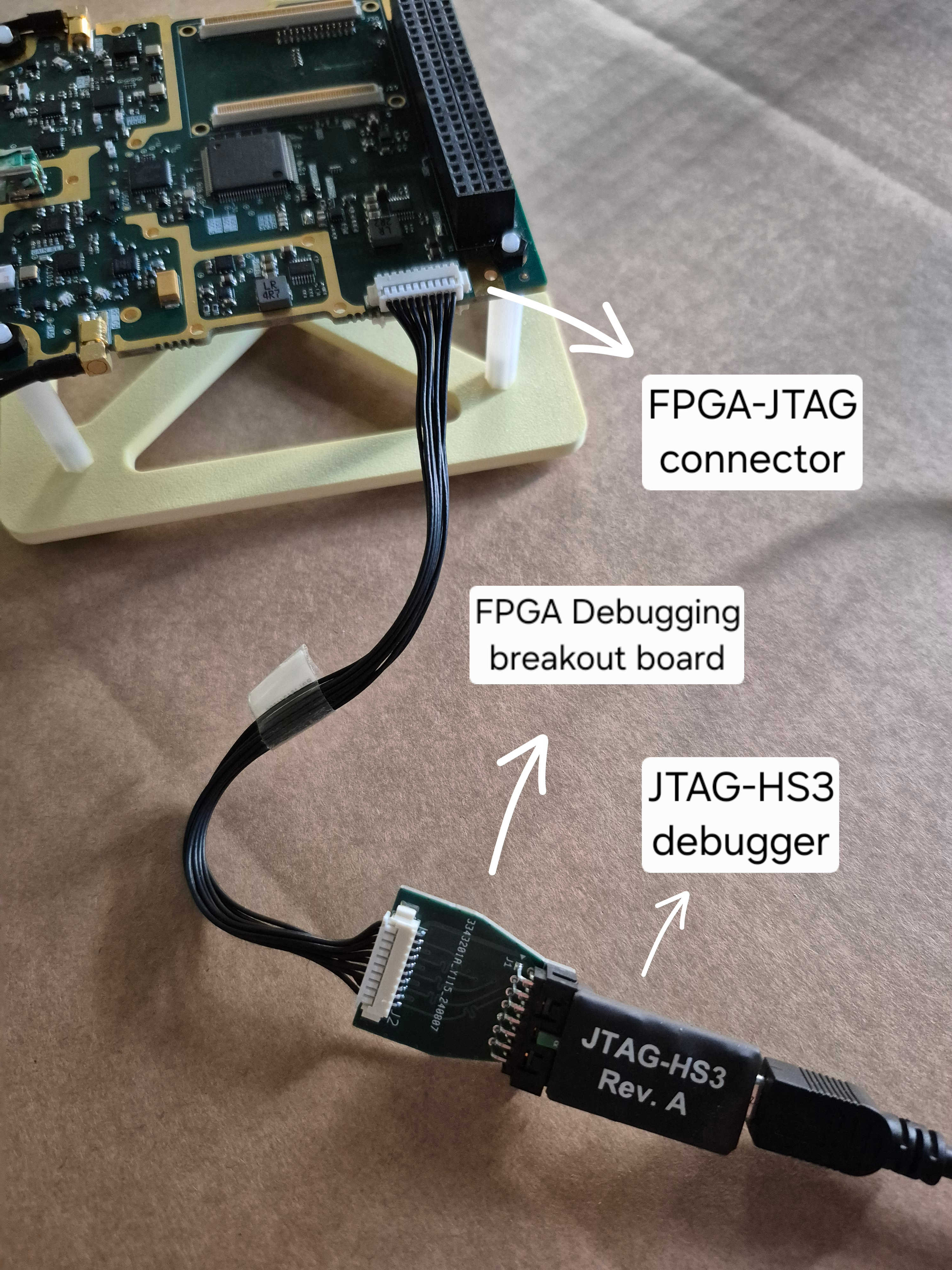
A 10-pin connector "FPGA-JTAG" (53261-1071) is located on the top right side of the board for the debugging and programming of the Alinx ZYNQ-7000 SOM XC7Z020 board. as described in the Interface control document. Various devices that support JTAG programming can be used. Similarly to the MCU programming a cable assembly (151341002) is used, of which one side is connected to the "FPGA-JTAG" connector and the other side to the FPGA Programming Breakout Board. This breakout board is connected to a 14-pin JTAG debugger, for example JTAG-HS3 or XILINX Platform Cable USB with the help of a ribbon cable.
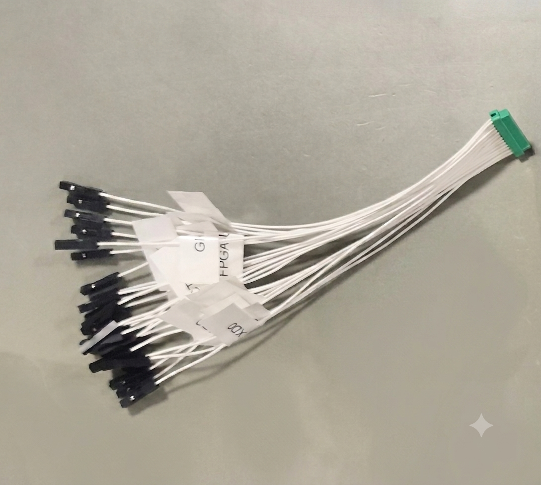
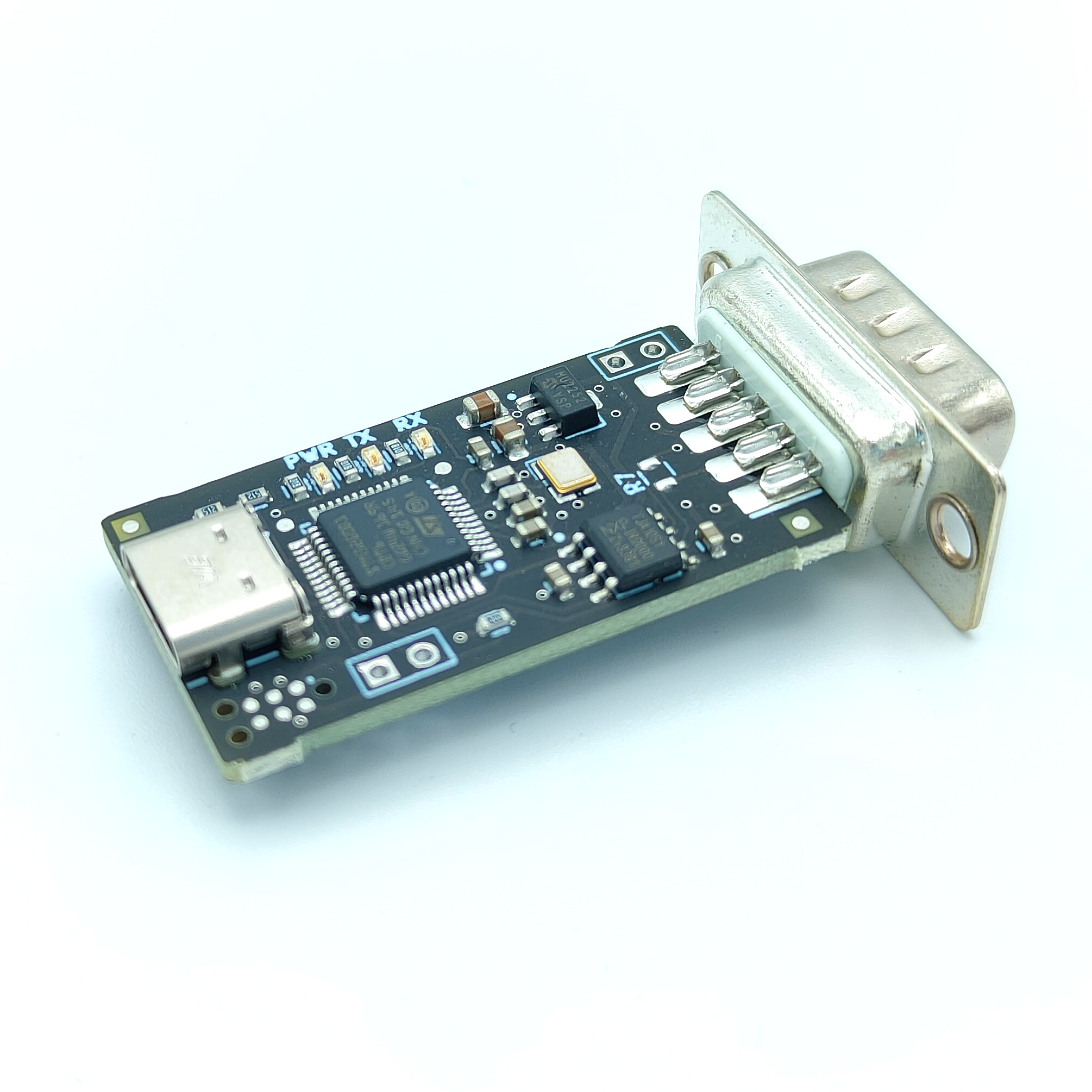
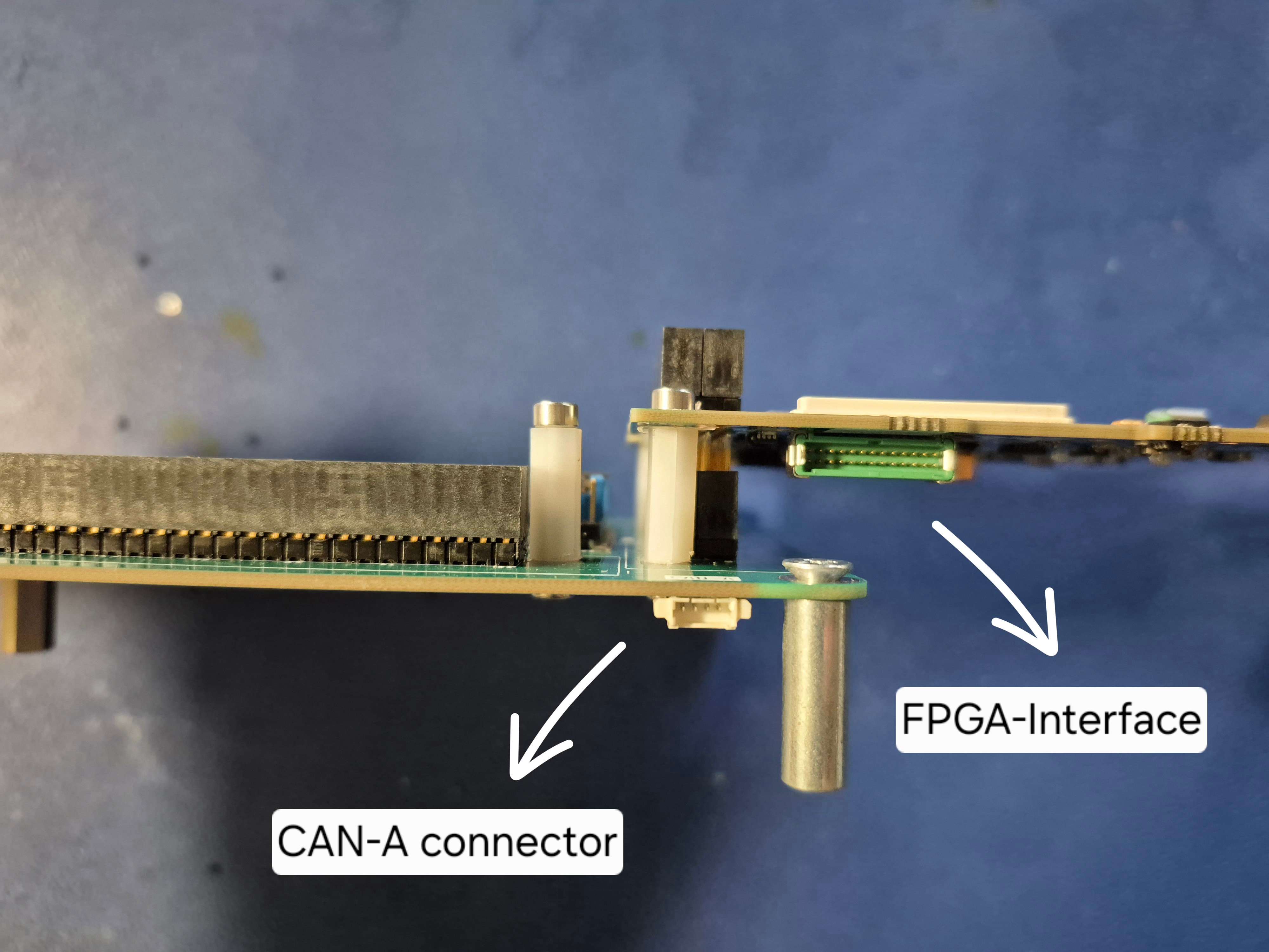
A 26-pin connector "FPGA-INTERFACE" (G125-MH12605L3R is located on the bottom left side of the board which exposes the UART and ethernet connection of the FPGA SOM and the eMMC present on the board. A custom cable assembly is required which exposes the connector interface to individual dupont-style female housing.
The ethernet wires are typically connected to the corresponding pins of the DP83867ERGZ RGMII 1000M/100M/10M Ethernet PHY evaluation module or to another subsystem which utilizes an ethernet connection.
The UART wires can be connected to a typical UART to USB device such as FT232 board.
The eMMC wires can be connected to an SD sniffer board such as (SparkFun™ microSD Sniffer) or custom made eMMC Sniffer. By default, the eMMC sniffer is used and thus the appropriate wires are crimped and inserted to an 8-pin picoblade (51021-0800) socket. For this use, the direction of the eMMC must point to the external (EXT) connector.
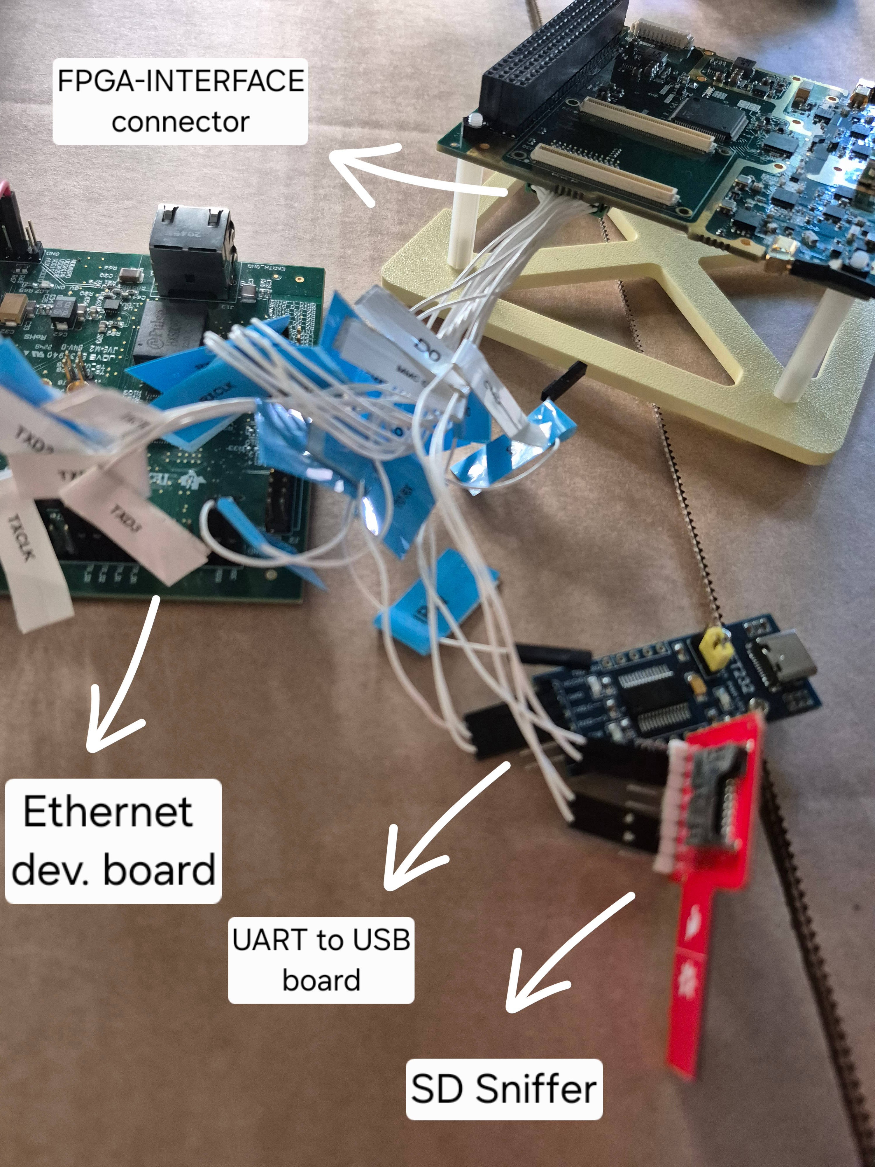
The complete setup is presented in the image below. Here 50Ω RF loads are used in the RF connection.
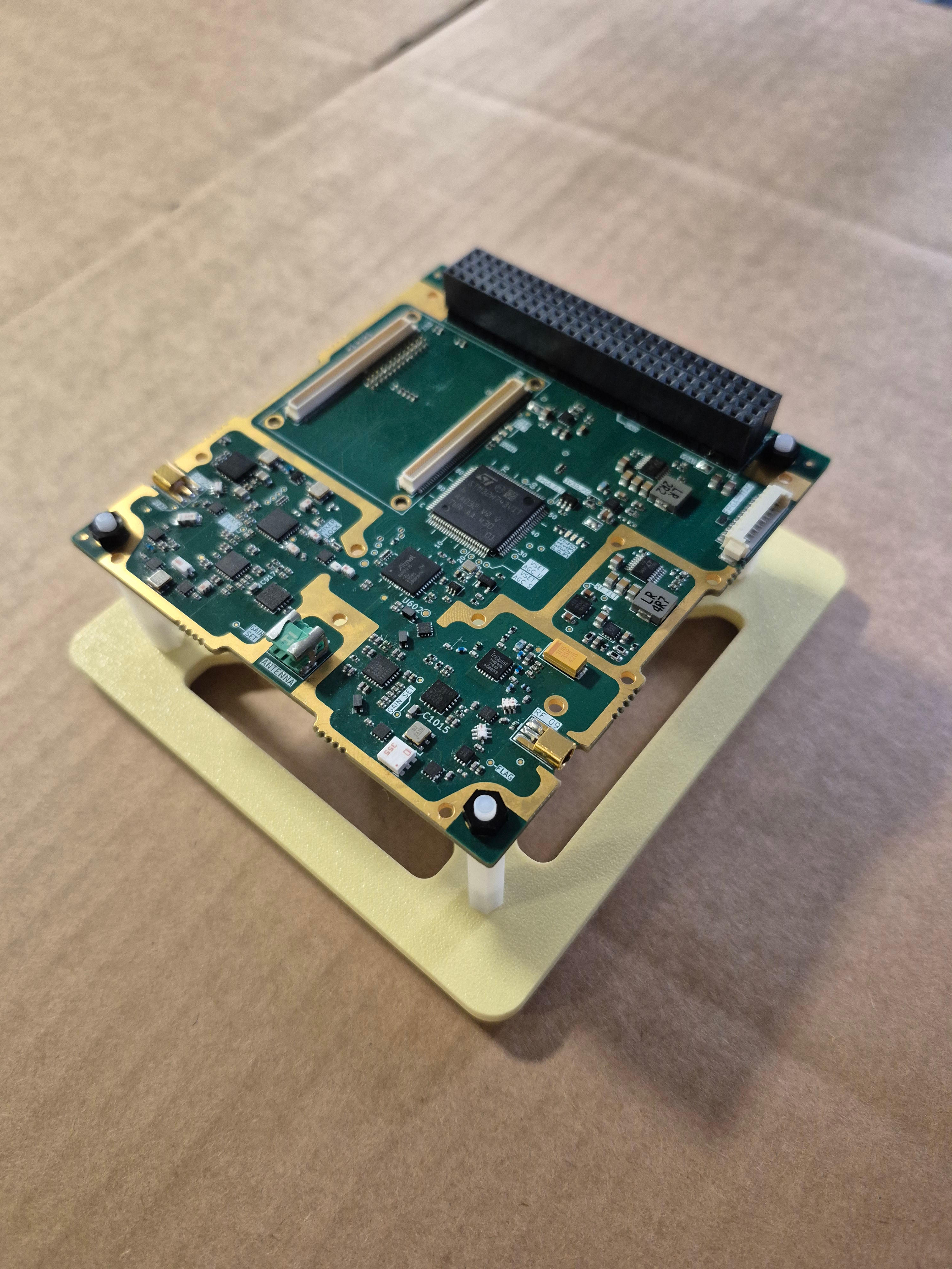
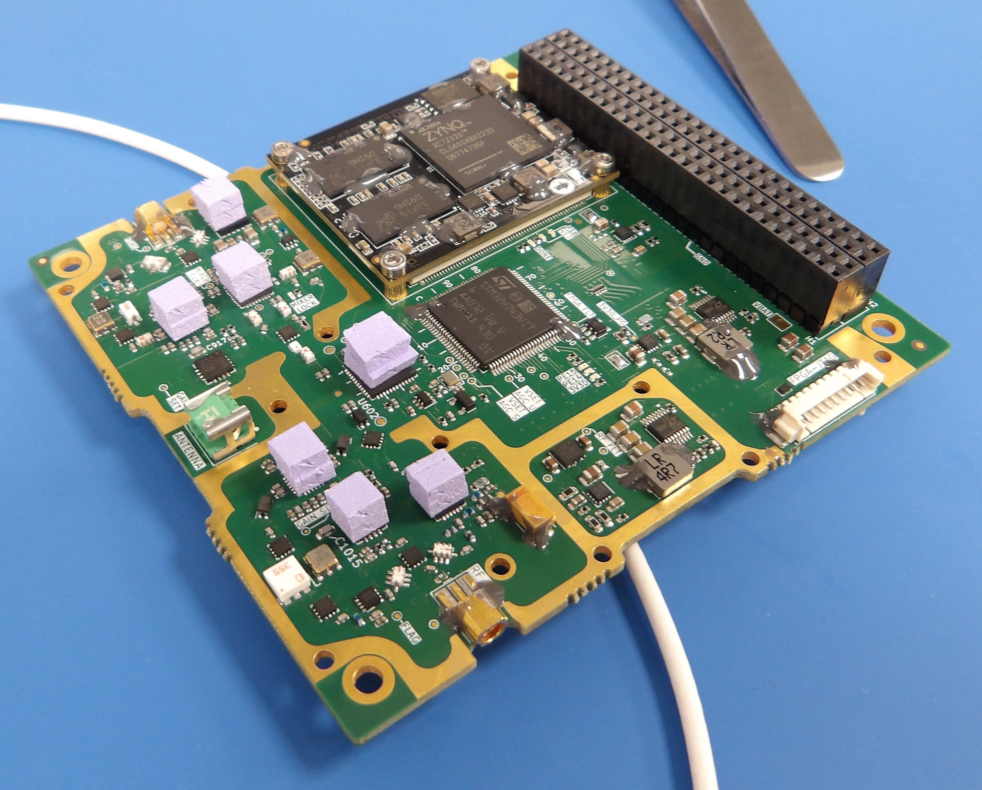
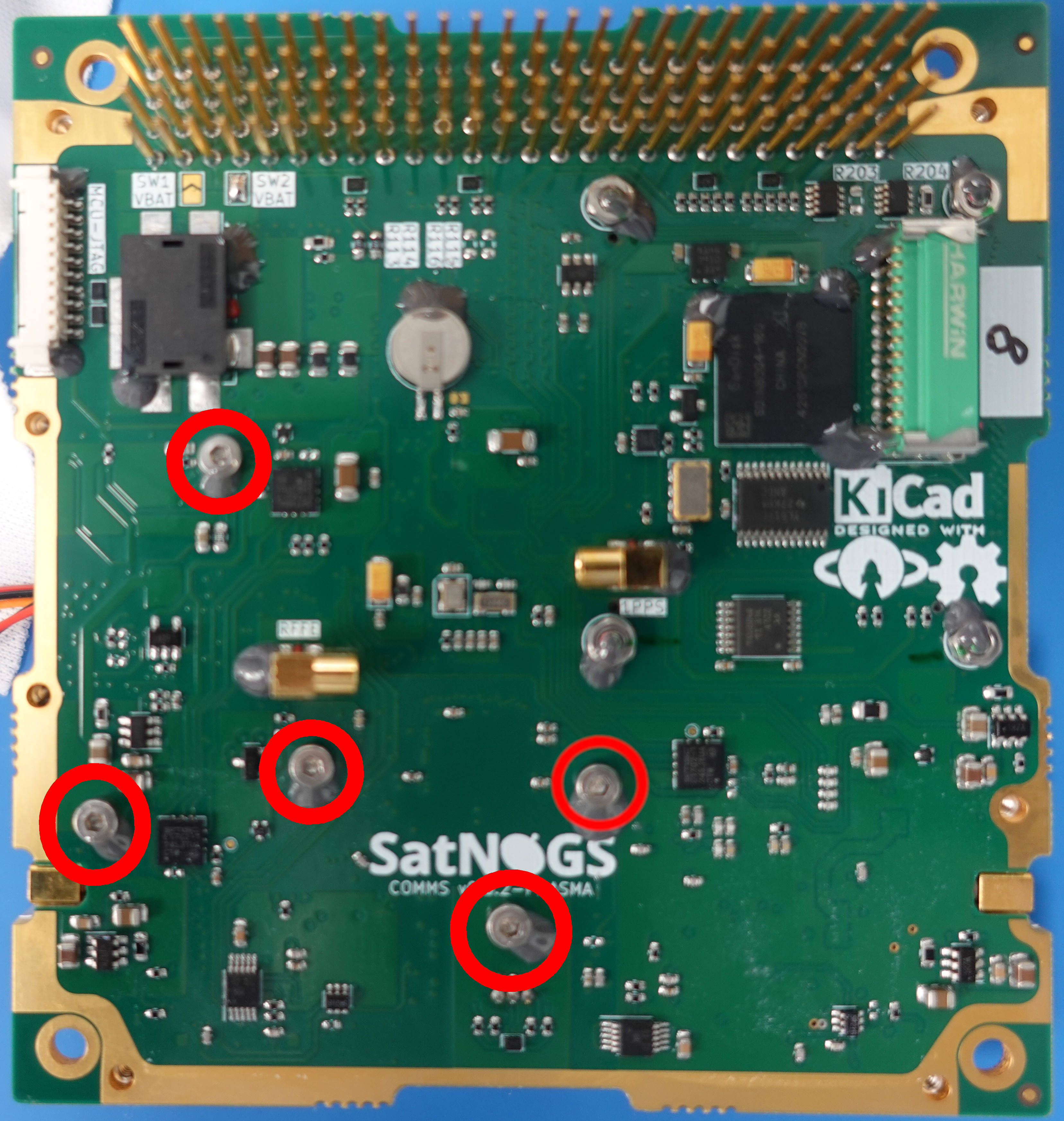
The FPGA of the SatNOGS COMMS board is available as a System-on-Module (SoM). Specifically the Alinx ZYNQ-7000 SoM XC7Z020, is used. This board is mounted on two AXK6A2337YG connectors by using four (4) M2-L3 F-F knurled brass spacer, four (4) M2-L8 (DIN912) bolts and four (4) M2 (DIN934) nuts.
| FPGA captured from the top side | FPGA captured from the side | Bottom side of the PCB. The bolts tightened with nuts are highlighted in red circles. |
| Figure 14: FPGA hardware inspection and mounting layout. | ||
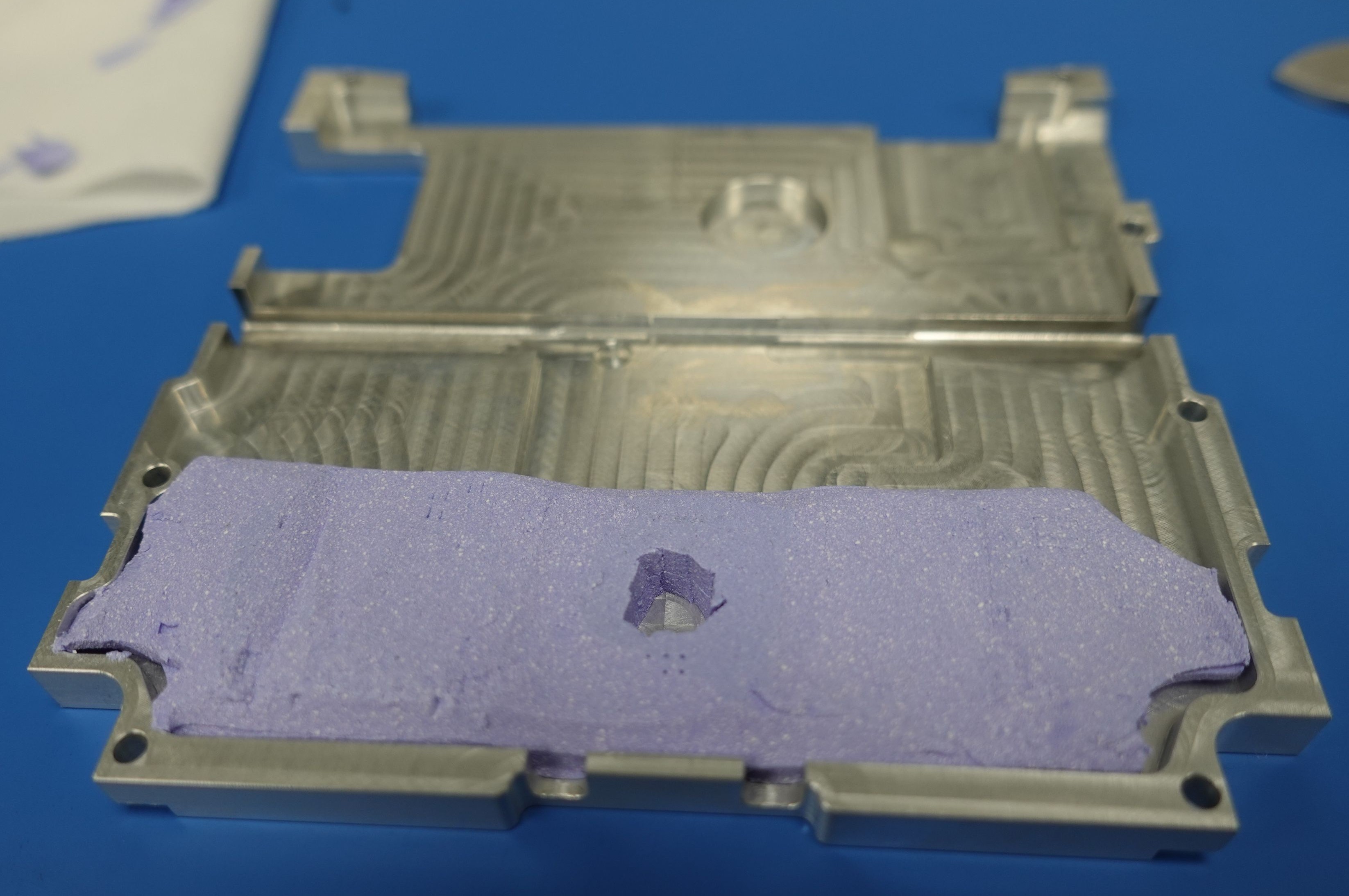
Staking provides mechanical support and protects components from vibrations and shocks experienced during launch and operation. It is usually added to heavy components, such as inductors and connectors, large chips, and screws/bolts which require strength support. The epoxy adhesive used on SatNOGS COMMS is 3M™ Scotch-Weld™ Epoxy Adhesive 2216 B/A Gray.
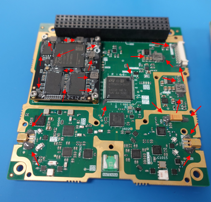
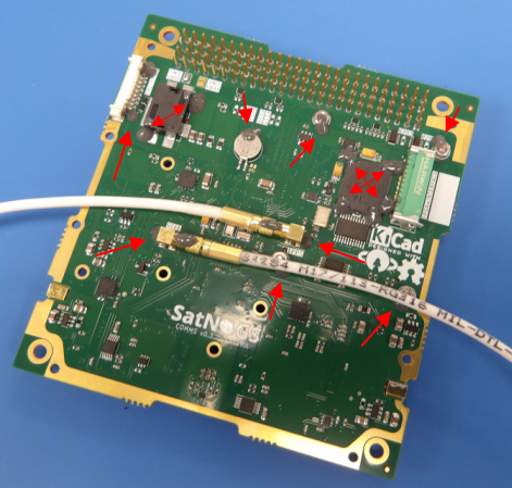
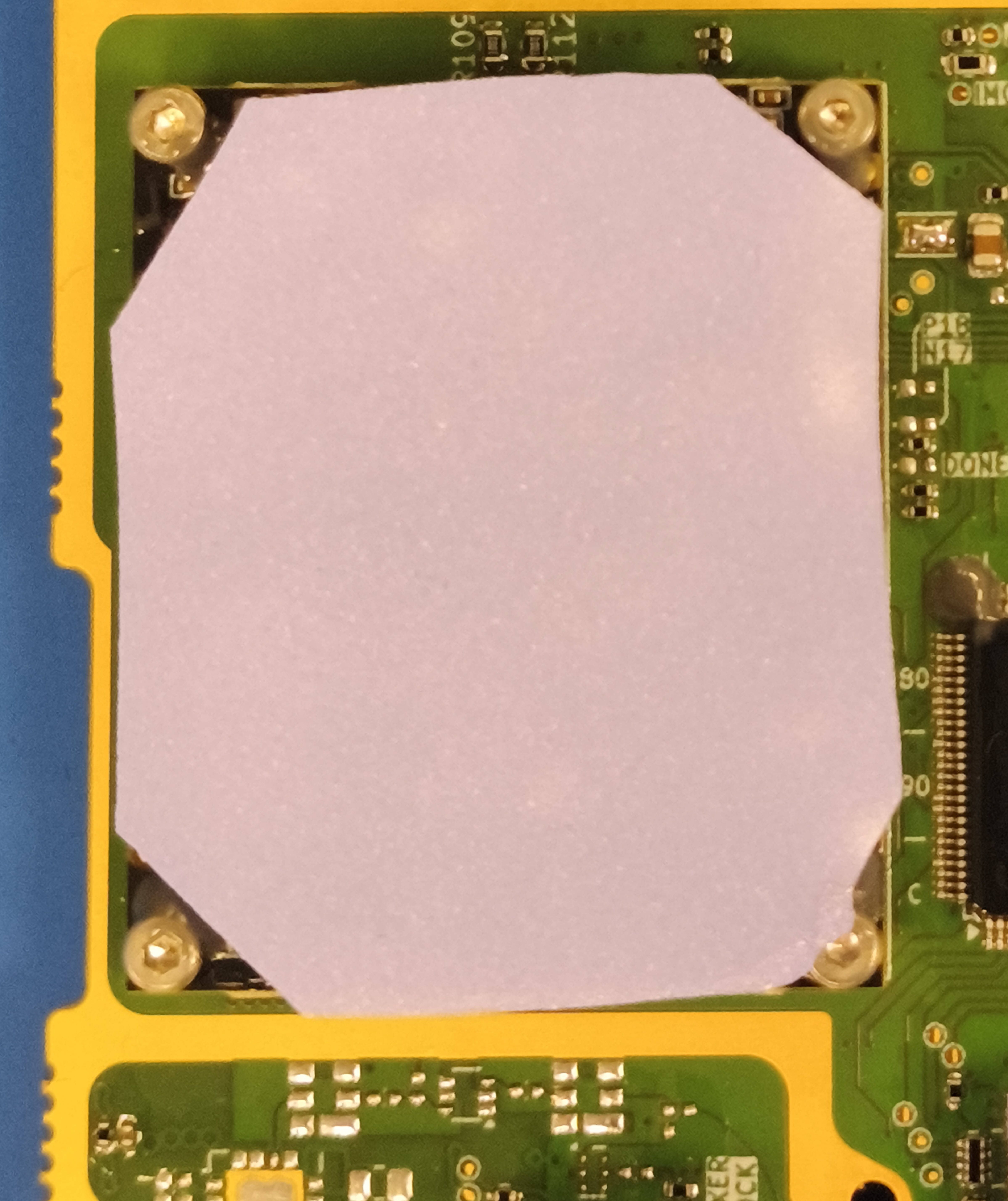
Before staking, the board should be properly cleaned with isopropyl alcohol 99% using an antistatic brush and cleaning cloth. A simple cleanliness level inspection could be performed by lighting with UV light. Afterward, the preparation of the adhesive should begin. Usually, a small plastic cup is used for the placement and mixing of the adhesive. The cup is placed on a precise scale to measure the amount of constituents used for mixing. The preparation and use guide of the adhesive can be found on the datasheet provided by the manufacturer. The adhesive is then applied on the recommended positions indicated by the red arrows in Figure 15 and Figure 16, with the help of a glue applicator. Staking should be applied to a minimum of 25% of the components' body height.
For more information, refer to IPC-J STD-001. After application, the adhesive should cure under the conditions (time and temperature) provided by the manufacturer. Finally, a record should be created for traceability purposes. The record should contain information such as the adhesive supplier's part number, date of first unsealing, expiration date, date of mixture, mixing ratio, cure temperature and time, photographs and all the actions performed leading to the final result.
Conformal coating acts as a shield against environmental hazards, protecting the circuitry from moisture, dust, radiation, and temperature extremes. Coating may not be necessary if the storage and operating conditions are optimal. An example of such conditions is the storage of the board in a dry cabinet with controlled temperature and humidity. Recommendations on conformal coatings are 422B Silicone Modified Conformal Coating, although no outgassing data exist and NuSil CV 1152, which does have outgassing data and is usually recommended in space applications in which outgassing of materials has a high chance of leading to degradation of other devices and components. Coating can be applied by spraying, or brushing. If coating is applied, it should be avoided on specific areas and components to prevent interference with their proper operation. These include connectors, exposed ground planes, and mechanical components. These components and areas should be properly defined and masked before coating application begins. Usually a peelable coating mask is applied. The necessary coating thickness should be defined according to IPC-J-STD-001.
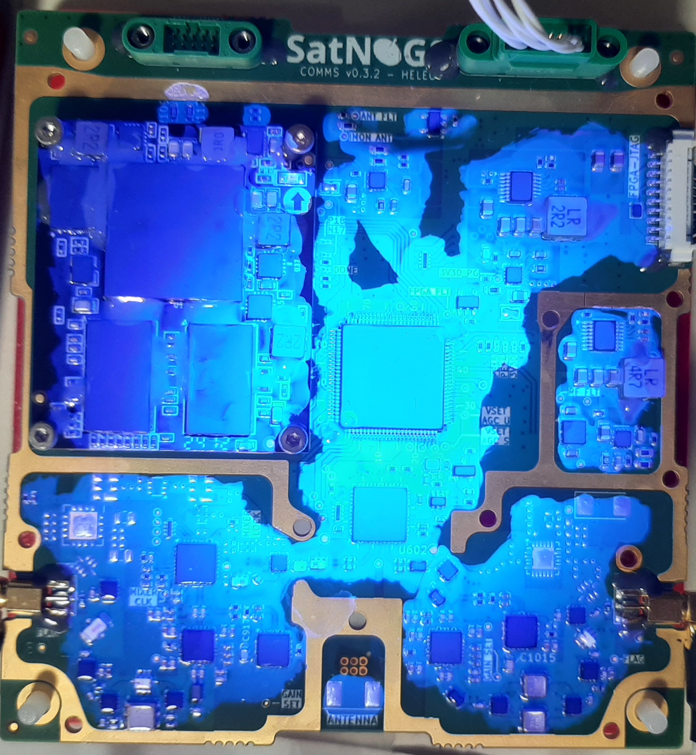
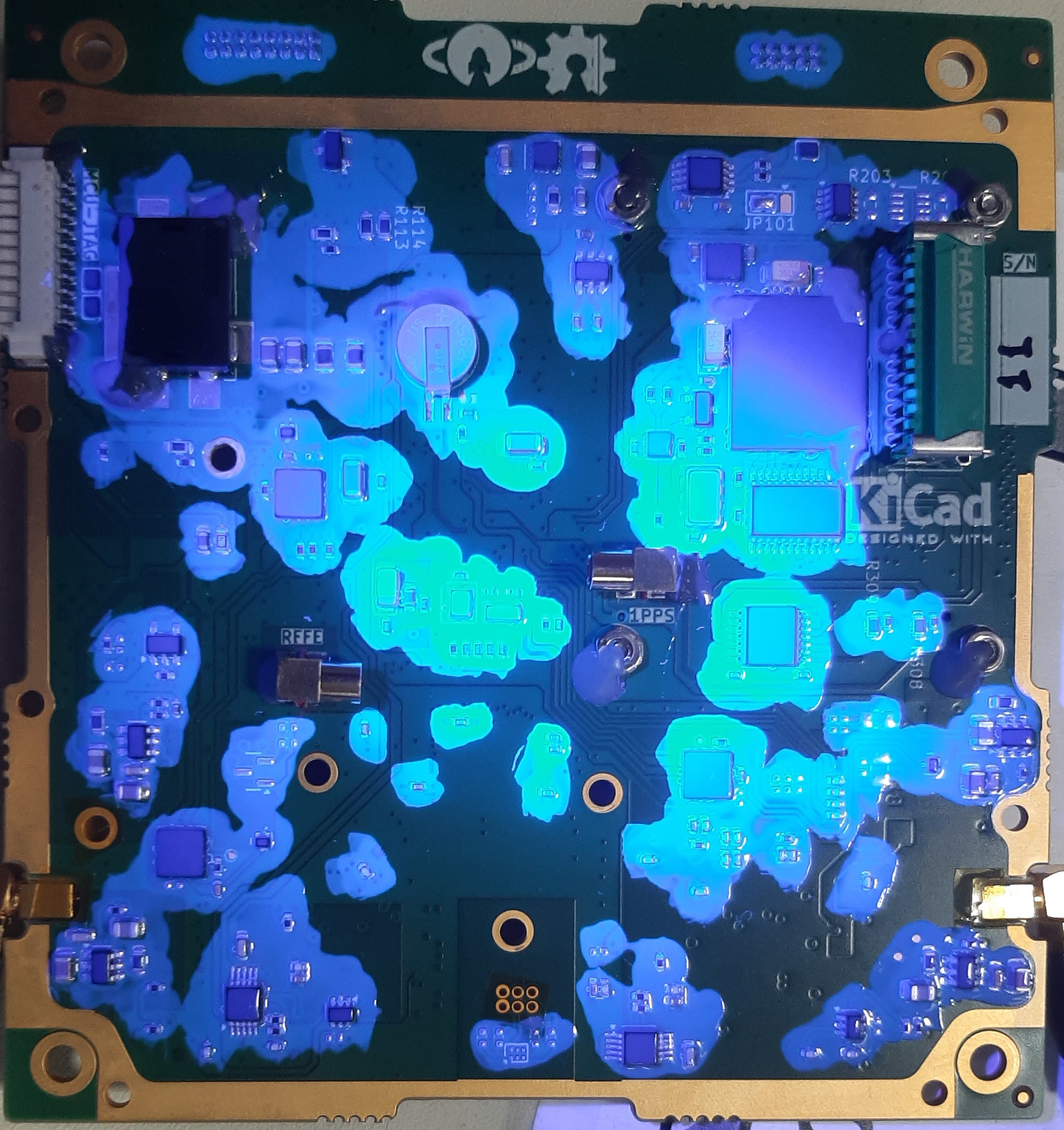
Before coating application, tests shall be performed to determine the required amount of coating to achieve the desired thickness. For example, when a spray coating is used, the number of passes that are necessary to reach the spec- ified thickness should be evaluated and recorded. To ensure consistent results, refer to the logs, each time a board is coated. After coating is applied, the board should be inspected using UV light to ensure that areas of interest have been adequately covered. The coating should then be cured in conditions according to the manufacturer’s datasheet specification. Conditions and results should be recorded for future reference. After curing, the board should be inspected again. If the coating application is satisfactory, the peelable mask may be removed. Photographs should be taken at each step of the procedure. Examples of coating applied on SatNOGS COMMS are shown in Figure 17 and Figure 18.
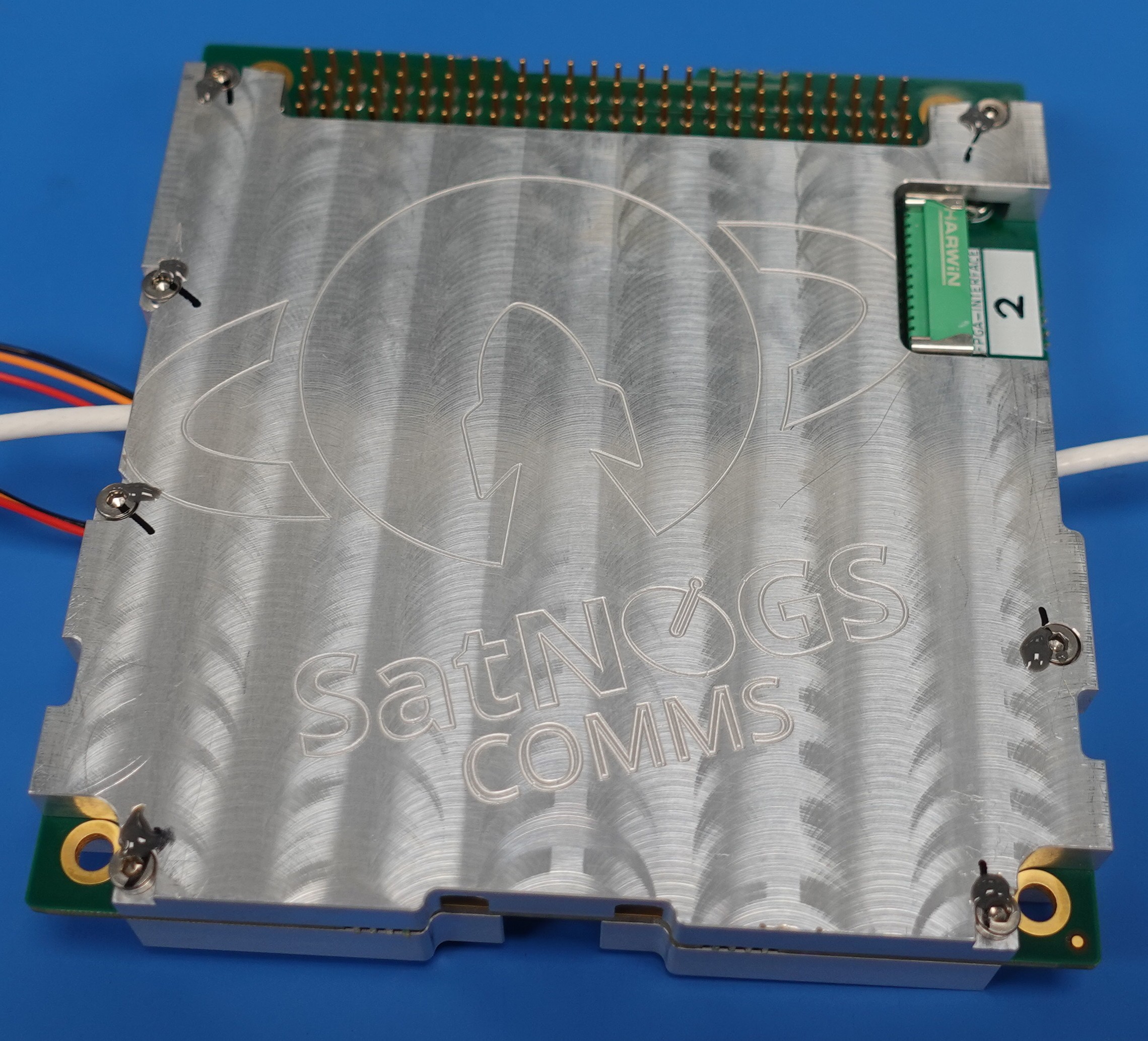
The EMI shield protects the board from unwanted external emission that could lead to performance degradation. In addition, it protects nearby subsystems from potential radiated emissions.
There are two EMI shields installed. The top and the bottom. The design files can usually be found on the release files of a particular version as step files. The shields should be thoroughly cleaned with 99% isopropyl alcohol. Before installation, the user should first connect the external clock reference cables, if required. They are referenced as RFFE' and 1PPS' and are located on the bottom side of the board. An example of cable placement can be seen in figure~fig:bot-stake}. If required, an EMI gasket, for example Laird™ 8863-0184-72, should be placed on the top shield. The purpose of the EMI gasket is to increase the effect of shielding and create a continuous conductive path, especially on the edges and slots between the board and the shield. Placement of the gasket can be seen in Figure 19. The strip should be cut between the screw holes.
Furthermore, in order to increase thermal transfer between the board and the shields, and thus reduce heating and temperature rise of the board, thermal gap fillers should be placed on areas that have increased temperature during operation. These areas include both the RF front-ends and especially the power amplifiers ICs. The thickness should be carefully chosen so that the thermal gap fillers make contact with the ICs of interest and the shield. If required, they can be cut stacked to reach the required size and thickness. Gap fillers used are the Laird™ A14418 or A17820/A17852 for improved outgassing. For the FPGA, bottom RF side and RF ICs a thermal gap filler of 1.0mm, 1.27mm and 2.54mm should be used.
On the top side, two gap fillers are cut and stacked on each top of the AT86RF215 transceiver, S-Band and UHF power amplifiers, AGCs and VGAs, and S-Band mixer. On the bottom side, a solid gap filler is placed to cover all the RF front-end area. Examples can be seen in Figure 21 and Figure 22. In addition, if the FPGA is operated intensely, it is encouraged to add a thermal gap filler to its entire surface facing the top shield, as seen in Figure 20. First, the top shield is installed by aligning and placing it on the top side of the board. There are five (5) M2 holes on the inner side of the top shield which are present to secure the EMI sensitive areas of the top shield to the board. Five (5) M2-L8-DIN912 bolts should be used for that purpose. If the shield is intended to be permanently installed, then a thread-locker should be applied on the bolts. The recommended thread-locker is the Vibra-Tite VC3. The bolts should be first placed on the inner holes and gently turned to ensure proper alignment. The bolts should then be tightened with a torque wrench. The recommended torque is 0.25 Nm. Finally, staking should be applied to the bolts following the instructions mentioned in Section~staking}.
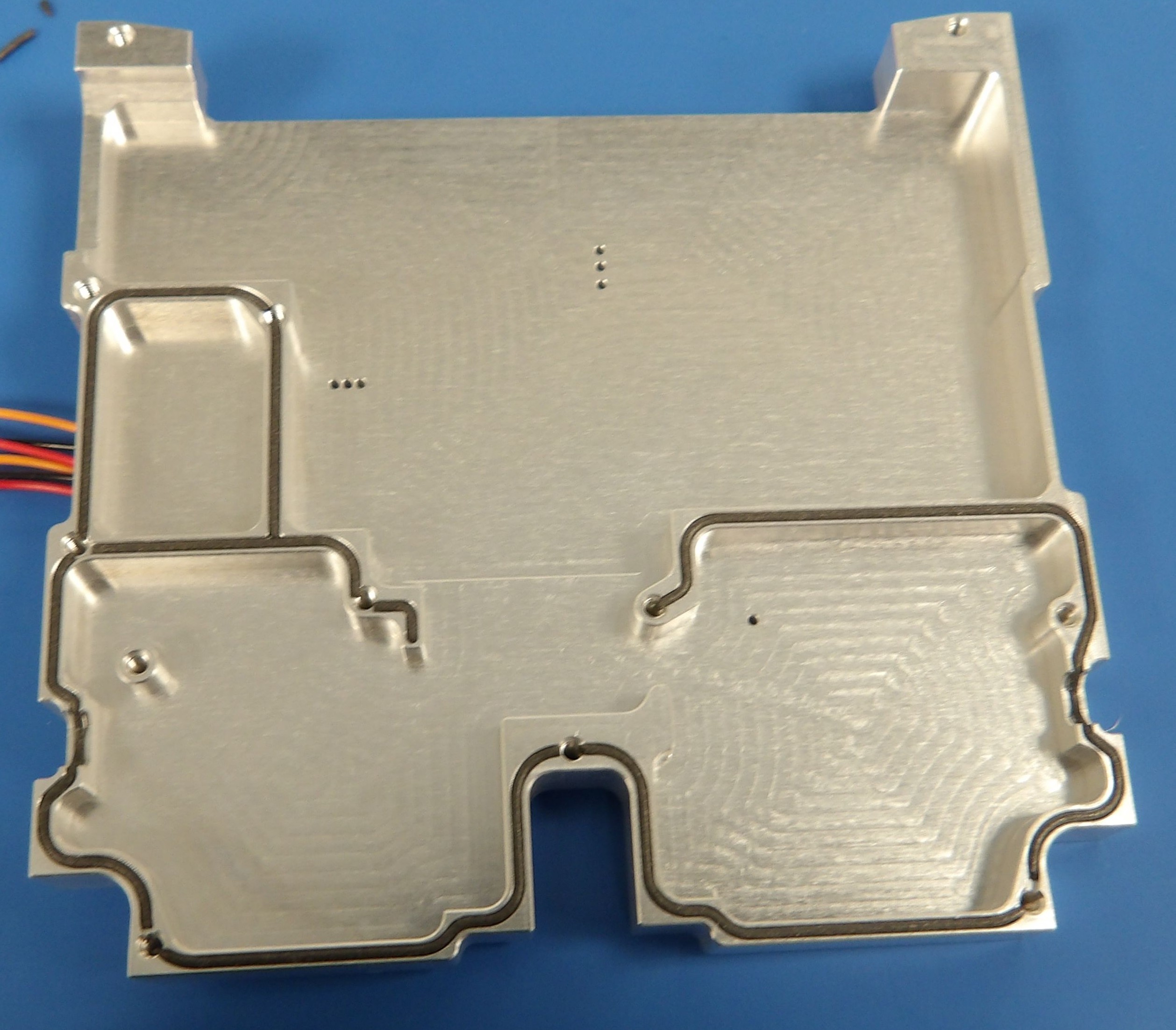
After the installation of the top shield, the bottom shield should be aligned and placed on the bottom side of the board. There are seven (7) M2 holes on the edges of the shield. Seven (7) M2-L10-DIN912 bolts should be used. Similarly to the top shield, if the shield is intended to be permanently installed, then a thread-locker should be applied on the bolts. The bolts should then be placed and gently turned to ensure proper alignment. Then, with the help of a torque wrench, they should be tightened with a recommended torque of 0.25 Nm. Staking should be applied on the bolts by following the instructions mentioned in Section~staking}.
Photographs should be taken on each step to log and document the procedure and results for future reference.
A table of the mechanical specifications and materials, used in the process of enclosing the SatNOGS COMMS board, is presented.
| Table 1: Mechanical specifications | ||||
| Use | Material | Part number | Quantity | Notes |
|---|---|---|---|---|
| FPGA | Bolt | M2-L8 DIN912 | 4 | Recommended torque: 0.25Nm |
| Nut | M2 DIN934 | 4 | - | |
| Spacer | M2-L3 F-F knurled brass spacer | 4 | - | |
| Top Shield | Bolt | M2 DIN934 | 7 | Recommended torque: 0.25Nm |
| EMI Gasket | Laird™ 8863-0184-72 | ~ 30cm | - | |
| Thermal gap filler for FPGA | Laird™ A17820-04 | According to fig_top-pads | Alternative: Laird™ A17752-04 Alternative with worse outgassing data: Laird™ A14418-04 Thickness: 1.00mm | |
| Thermal gap filler for RF ICs | Laird™ A17820-10 | According to fig_top-pads | Alternative: Laird™ A17752-10 Alternative with worse outgassing: Laird™ A14418-10 Thickness: 2.54mm | |
| Bottom Shield | Bolt | M2-L8 DIN912 | 5 | Recommended torque: 0.25Nm |
| Thermal gap filler for RF front-end | Laird™ A17820-05 | According to fig_bot-pads | Alternative: Laird™ A17752-05 Alternative with worse outgassing: Laird™ A14418-05 Thickness: 1.27mm | |
| PCB | Conformal coating | Nusil™ CV 1152 | According to fig_bottom-coating & fig_top-coating | Alternative with worse outgassing: MG Chemicals™ 422B |